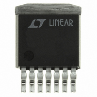
LT1506CR-SYNC Linear Technology, LT1506CR-SYNC Datasheet - Page 6

LT1506CR-SYNC
Manufacturer Part Number
LT1506CR-SYNC
Description
IC SW REG STEP-DOWN 500KHZ 7-DD
Manufacturer
Linear Technology
Type
Step-Down (Buck)r
Datasheet
1.LT1506CS8-3.3PBF.pdf
(24 pages)
Specifications of LT1506CR-SYNC
Internal Switch(s)
Yes
Synchronous Rectifier
No
Number Of Outputs
1
Voltage - Output
Adjustable
Current - Output
4.5A
Frequency - Switching
500kHz
Voltage - Input
4 ~ 15 V
Operating Temperature
0°C ~ 125°C
Mounting Type
Surface Mount
Package / Case
D²Pak, TO-263 (7 leads + tab)
Lead Free Status / RoHS Status
Contains lead / RoHS non-compliant
Power - Output
-
Available stocks
Company
Part Number
Manufacturer
Quantity
Price
Part Number:
LT1506CR-SYNC
Manufacturer:
LINEAR/凌特
Quantity:
20 000
Part Number:
LT1506CR-SYNC#TRPBF
Manufacturer:
LINEAR/凌特
Quantity:
20 000
LT1506
PIN
FB/SENSE: The feedback pin is used to set output voltage
using an external voltage divider that generates 2.42V at
the pin with the desired output voltage. The fixed voltage
(-3.3) parts have the divider included on the chip and the
FB pin is used as a SENSE pin, connected directly to the
3.3V output. Three additional functions are performed by
the FB pin. When the pin voltage drops below 1.7V, switch
current limit is reduced. Below 1.5V the external sync
function is disabled. Below 1V, switching frequency is also
reduced. See Feedback Pin Function section in Applica-
tions Information for details.
BOOST: The BOOST pin is used to provide a drive voltage,
higher than the input voltage, to the internal bipolar NPN
power switch. Without this added voltage, the typical
switch voltage loss would be about 1.5V. The additional
boost voltage allows the switch to saturate and voltage
loss approximates that of a 0.07 FET structure, but with
much smaller die area. Efficiency improves from 75% for
conventional bipolar designs to > 89% for these new parts.
V
This pin powers the internal circuitry and internal regula-
tor. At NPN switch on and off, high dI/dt edges occur on
this pin. Keep the external bypass and catch diode close to
this pin. All trace inductance on this path will create a
voltage spike at switch off, adding to the V
across the internal NPN.
GND: The GND pin connection needs consideration for
two reasons. First, it acts as the reference for the regulated
output, so load regulation will suffer if the “ground” end of
the load is not at the same voltage as the GND pin of the
IC. This condition will occur when load current or other
currents flow through metal paths between the GND pin
and the load ground point. Keep the ground path short
between the GND pin and the load and use a ground plane
when possible. The second consideration is EMI caused
by GND pin current spikes. Internal capacitance between
the V
6
IN
U
: This is the collector of the on-chip power NPN switch.
SW
FUNCTIONS
pin and the GND pin creates very narrow (<10ns)
U
U
CE
voltage
current spikes in the GND pin. If the GND pin is connected
to system ground with a long metal trace, this trace may
radiate excess EMI. Keep the path between the input
bypass and the GND pin short. The GND pin of the SO-8
package is directly attached to the internal tab. This pin
should be attached to a large copper area to improve
thermal resistance.
V
NPN switch. This pin is driven up to the input pin voltage
during switch on time. Inductor current drives the switch
pin negative during switch off time. Negative voltage is
clamped with the external catch diode. Maximum negative
switch voltage allowed is – 0.8V.
SYNC: The sync pin is used to synchronize the internal
oscillator to an external signal. It is directly logic compat-
ible and can be driven with any signal between 10% and
90% duty cycle. The synchronizing range is equal to initial
operating frequency, up to 1MHz. This pin replaces SHDN
on -SYNC option parts. See Synchronizing section in
Applications Information for details. When not in use, this
pin should be grounded.
SHDN: The shutdown pin is used to turn off the regulator
and to reduce input drain current to a few microamperes.
Actually, this pin has two separate thresholds, one at
2.38V to disable switching, and a second at 0.4V to force
complete micropower shutdown. The 2.38V threshold
functions as an accurate undervoltage lockout (UVLO).
This is sometimes used to prevent the regulator from
operating until the input votlage has reached a predeter-
mined level.
V
input of the peak switch current comparator. It is normally
used for frequency compensation, but can do double duty
as a current clamp or control loop override. This pin sits
at about 1V for very light loads and 2V at maximum load.
It can be driven to ground to shut off the regulator, but if
driven high, current must be limited to 4mA.
SW
C
: The V
: The switch pin is the emitter of the on-chip power
C
pin is the output of the error amplifier and the


