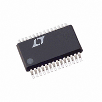
LTC3728LEGN Linear Technology, LTC3728LEGN Datasheet - Page 18

LTC3728LEGN
Manufacturer Part Number
LTC3728LEGN
Description
IC REG SW DUAL 2PH STPDWN 28SSOP
Manufacturer
Linear Technology
Series
PolyPhase®r
Type
Step-Down (Buck)r
Datasheet
1.LTC3728LXCUHPBF.pdf
(36 pages)
Specifications of LTC3728LEGN
Internal Switch(s)
No
Synchronous Rectifier
Yes
Number Of Outputs
2
Voltage - Output
0.8 ~ 7 V
Current - Output
3A
Frequency - Switching
250kHz ~ 550kHz
Voltage - Input
4.5 ~ 28 V
Operating Temperature
-40°C ~ 85°C
Mounting Type
Surface Mount
Package / Case
28-SSOP
Lead Free Status / RoHS Status
Contains lead / RoHS non-compliant
Power - Output
-
Available stocks
Company
Part Number
Manufacturer
Quantity
Price
Company:
Part Number:
LTC3728LEGN
Manufacturer:
LINEAR
Quantity:
84
Part Number:
LTC3728LEGN
Manufacturer:
LINEAR
Quantity:
20 000
Company:
Part Number:
LTC3728LEGN#2CQPBF
Manufacturer:
LT
Quantity:
3 048
Company:
Part Number:
LTC3728LEGN#PBF
Manufacturer:
KEC
Quantity:
1 130
Part Number:
LTC3728LEGN#PBF
Manufacturer:
LINEAR/凌特
Quantity:
20 000
Company:
Part Number:
LTC3728LEGN#TRPBF
Manufacturer:
LT
Quantity:
3 048
Part Number:
LTC3728LEGN#TRPBF
Manufacturer:
LT/凌特
Quantity:
20 000
Company:
Part Number:
LTC3728LEGN-1#PBF
Manufacturer:
LT
Quantity:
189
APPLICATIONS INFORMATION
LTC3728L/LTC3728LX
where δ is the temperature dependency of R
R
at the MOSFET’s Miller threshold voltage. V
typical MOSFET minimum threshold voltage.
Both MOSFETs have I
equation includes an additional term for transition losses,
which are highest at high input voltages. For V
the high current effi ciency generally improves with larger
MOSFETs, while for V
increase to the point that the use of a higher R
with lower C
synchronous MOSFET losses are greatest at high input
voltage when the top switch duty factor is low or during
a short-circuit when the synchronous switch is on close
to 100% of the period.
The term (1 + δ) is generally given for a MOSFET in the
form of a normalized R
δ = 0.005/°C can be used as an approximation for low
voltage MOSFETs.
The Schottky diode, D1, shown in Figure 1 conducts during
the dead time between the conduction of the two power
MOSFETs. This prevents the body diode of the bottom
MOSFET from turning on, storing charge during the dead
time and requiring a reverse-recovery period that could
cost as much as 3% in effi ciency at high V
Schottky is generally a good compromise for both regions
of operation due to the relatively small average current.
Larger diodes result in additional transition losses due to
their larger junction capacitance.
C
The selection of C
chitecture and its impact on the worst-case RMS current
drawn through the input network (battery/fuse/capacitor).
It can be shown that the worst-case RMS current occurs
when only one controller is operating. The controller
with the highest (V
in the subsequent formula to determine the maximum
RMS current requirement. Increasing the output current,
drawn from the other out-of-phase controller, will actually
decrease the input RMS ripple current from this maximum
value (see Figure 4). The out-of-phase technique typically
reduces the input capacitor’s RMS ripple current by a
18
IN
DR
and C
(approximately 4Ω) is the effective driver resistance
OUT
MILLER
Selection
IN
actually provides higher effi ciency. The
OUT
2
IN
R losses while the topside N-channel
is simplifi ed by the multiphase ar-
)(I
DS(ON)
> 20V the transition losses rapidly
OUT
) product needs to be used
vs Temperature curve, but
IN
TH(MIN)
DS(ON)
. A 1A to 3A
DS(ON)
IN
device
< 20V
is the
and
factor of 30% to 70% when compared to a single phase
power supply solution.
The type of input capacitor, value and ESR rating have
effi ciency effects that need to be considered in the selec-
tion process. The capacitance value chosen should be
suffi cient to store adequate charge to keep high peak
battery currents down. 20μF to 40μF is usually suffi cient
for a 25W output supply operating at 200kHz. The ESR of
the capacitor is important for capacitor power dissipation
as well as overall battery effi ciency. All of the power (RMS
ripple current • ESR) not only heats up the capacitor but
wastes power from the battery.
Medium voltage (20V to 35V) ceramic, tantalum, OS-CON
and switcher-rated electrolytic capacitors can be used
as input capacitors, but each has drawbacks: ceramic
voltage coeffi cients are very high and may have audible
piezoelectric effects; tantalums need to be surge-rated;
OS-CONs suffer from higher inductance, larger case size
and limited surface-mount applicability; electrolytics’
higher ESR and dryout possibility require several to be
used. Multiphase systems allow the lowest amount of
capacitance overall. As little as one 22μF or two to three
10μF ceramic capacitors are an ideal choice in a 20W to
35W power supply due to their extremely low ESR. Even
though the capacitance at 20V is substantially below their
rating at zero-bias, very low ESR loss makes ceramics
an ideal candidate for highest effi ciency battery operated
systems. Also consider parallel ceramic and high quality
electrolytic capacitors as an effective means of achieving
ESR and bulk capacitance goals.
In continuous mode, the source current of the top N-channel
MOSFET is a square wave of duty cycle V
large voltage transients, a low ESR input capacitor sized for
the maximum RMS current of one channel must be used.
The maximum RMS capacitor current is given by:
This formula has a maximum at V
= I
used for design because even signifi cant deviations do not
offer much relief. Note that capacitor manufacturer’s ripple
OUT
C
IN
/2. This simple worst-case condition is commonly
Required I
RMS
I
MAX
V
OUT
IN
(
= 2V
V
IN
OUT
V
IN
OUT
/V
V
OUT
IN
, where I
. To prevent
)
1/2
3728lxfe
RMS


