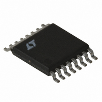
LT1976IFE#TR Linear Technology, LT1976IFE#TR Datasheet - Page 4

LT1976IFE#TR
Manufacturer Part Number
LT1976IFE#TR
Description
IC REG SW STEP DWN 1.5A 16-TSSOP
Manufacturer
Linear Technology
Type
Step-Down (Buck)r
Datasheet
1.LT1976IFEPBF.pdf
(28 pages)
Specifications of LT1976IFE#TR
Internal Switch(s)
Yes
Synchronous Rectifier
No
Number Of Outputs
1
Voltage - Output
1.2 ~ 54 V
Current - Output
1.5A
Frequency - Switching
200kHz
Voltage - Input
3.3 ~ 60 V
Operating Temperature
-40°C ~ 125°C
Mounting Type
Surface Mount
Package / Case
16-TSSOP Exposed Pad, 16-eTSSOP, 16-HTSSOP
Lead Free Status / RoHS Status
Contains lead / RoHS non-compliant
Power - Output
-
Available stocks
Company
Part Number
Manufacturer
Quantity
Price
operating temperature range, otherwise specifications are at T
FB/PGFB = 1.25V, C
LT1976/LT1976B
SYMBOL
I
I
I
V
I
V
Note 1: Stresses beyond those listed under Absolute Maximum Ratings
may cause permanent damage to the device. Exposure to any Absolute
Maximum Rating condition for extended periods may affect device
reliability and lifetime.
Note 2: The LT1976EFE/LT1976BEFE are guaranteed to meet performance
specifications from 0°C to 125°C junction temperature. Specifications over
the –40°C to 125°C operating junction temperature range are assured by
design, characterization and correlation with statistical process controls.
The LT1976IFE/LT1976BIFE/LT1976HFE are guaranteed and tested over
the full –40°C to 125°C operating junction temperature range. The
LT1976HFE is also tested to the LT1976HFE electrical characteristics table
at 140°C operating junction temperature. High junction temperatures
degrade operating lifetimes.
Note 3: Minimum input voltage is defined as the voltage where switching
starts. Actual minimum input voltage to maintain a regulated output will
depend upon output voltage and load current. See Applications
Information.
Note 4: Supply input current is the quiescent current drawn by the input
pin. Its typical value depends on the voltage on the BIAS pin and operating
state of the LT1976. With the BIAS pin at 0V, all of the quiescent current
required to operate the LT1976 will be provided by the V
BIAS voltage above its minimum input voltage, a portion of the total
quiescent current will be supplied by the BIAS pin. Supply sleep current
for the LT1976 is defined as the quiescent current during the “sleep”
portion of Burst Mode operation. See Applications Information for
determining application supply currents.
ELECTRICAL CHARACTERISTICS
4
PK
CSS
PGFB
CT
PGFB
CT
PARAMETER
SW Current Limit
Switch On Resistance (Note 9)
Switching Frequency
Maximum Duty Cycle
Minimum SYNC Amplitude
SYNC Frequency Range
SYNC Input Impedance
C
PGFB Input Current
PGFB Voltage Threshold (Note 11)
C
C
C
PG Leakage (Note 11)
PG Sink Current (Note 11)
SS
T
T
T
Source Current (Note 11)
Sink Current (Note 11)
Voltage Threshold (Note 11)
Current Threshold (Note 10)
SS
/SYNC = 0V unless otherwise noted.
IN
pin. With the
CONDITIONS
BOOST = OPEN
SYNC = 0.5V
PG = 12V
PGFB = 1V, PG = 400mV
The
J
●
= 25°C. V
denotes the specifications which apply over the full –40°C to 140°C
Note 5: Minimum BIAS voltage is the voltage on the BIAS pin when I
sourced into the pin.
Note 6: This is the minimum voltage across the boost capacitor needed to
guarantee full saturation of the internal power switch.
Note 7: Boost current is the current flowing into the BOOST pin with the
pin held 3.3V above input voltage. It flows only during switch on time.
Note 8: Gain is measured with a V
Note 9: Switch on resistance is calculated by dividing V
the forced current (1.5A LT1976, 1.2A LT1976B). See Typical Performance
Characteristics for the graph of switch voltage at other currents.
Note 10: The C
the C
See the Soft-Start section in Applications Information.
Note 11: The PGFB threshold is defined as the percentage of V
which causes the current source output of the C
sinking (below threshold) to sourcing current (above threshold). When
sourcing current, the voltage on the C
internally. When the clamp is activated, the output of the PG pin will be set
to a high impedance state. When the C
be set active low with a current sink capability of 200μA.
IN
SS
= 12V, SHDN = 12V, BOOST = 15.3V, BIAS = 5V,
pin which results in an increase in sink current from the V
SS
threshold is defined as the value of current sourced into
●
●
●
●
C
swing from 1.15V to 750mV.
MIN
1.16
150
230
120
1.5
T
90
87
7
1
T
pin rises until it is clamped
clamp is inactive the PG pin will
TYP
200
600
200
T
2.4
0.2
1.5
3.6
1.2
0.1
92
85
13
25
90
2
pin to change from
IN
to SW voltage by
MAX
1.26
260
100
0.6
2.0
5.5
20
93
1
REF
C
voltage
pin.
UNITS
BIAS
1976bfg
kHz
kHz
mA
kΩ
μA
nA
μA
μA
μA
%
%
Ω
is
A
V
V


