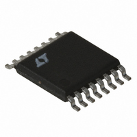
LT1976IFE#TR Linear Technology, LT1976IFE#TR Datasheet - Page 8

LT1976IFE#TR
Manufacturer Part Number
LT1976IFE#TR
Description
IC REG SW STEP DWN 1.5A 16-TSSOP
Manufacturer
Linear Technology
Type
Step-Down (Buck)r
Datasheet
1.LT1976IFEPBF.pdf
(28 pages)
Specifications of LT1976IFE#TR
Internal Switch(s)
Yes
Synchronous Rectifier
No
Number Of Outputs
1
Voltage - Output
1.2 ~ 54 V
Current - Output
1.5A
Frequency - Switching
200kHz
Voltage - Input
3.3 ~ 60 V
Operating Temperature
-40°C ~ 125°C
Mounting Type
Surface Mount
Package / Case
16-TSSOP Exposed Pad, 16-eTSSOP, 16-HTSSOP
Lead Free Status / RoHS Status
Contains lead / RoHS non-compliant
Power - Output
-
Available stocks
Company
Part Number
Manufacturer
Quantity
Price
LT1976/LT1976B
NC (Pins 1, 3, 5): No Connection. Pins 1, 3, 5 are
electrically isolated from the LT1976. They may be con-
nected to PCB traces to aid in PCB layout.
SW (Pin 2): The SW pin is the emitter of the on-chip power
NPN switch. This pin is driven up to the input pin voltage
during switch on time. Inductor current drives the SW pin
negative during switch off time. Negative voltage is clamped
with the external Schottky catch diode to prevent exces-
sive negative voltages.
V
switch. V
voltage on the BIAS pin is not present. High di/dt edges
occur on this pin during switch turn on and off. Keep the
path short from the V
capacitor, through the catch diode back to SW. All trace
inductance on this path will create a voltage spike at switch
off, adding to the V
BOOST (Pin 6): The BOOST pin is used to provide a drive
voltage, higher than the input voltage, to the internal
bipolar NPN power switch. Without this added voltage, the
typical switch voltage loss would be about 1.5V. The
additional BOOST voltage allows the switch to saturate
and its voltage loss approximates that of a 0.2Ω FET
structure, but with much smaller die area.
PI FU CTIO S
8
TYPICAL PERFOR A CE CHARACTERISTICS
IN
U
(Pin 4): This is the collector of the on-chip power NPN
IN
U
powers the internal control circuitry when a
CE
U
voltage across the internal NPN.
IN
pin through the input bypass
W
U
500mA/DIV
100mV/DIV
I
OUT
V
OUT
1A
0A
LT1976 Step Response
V
V
C
I
DC
IN
OUT
OUT
= 12V
= 250mA
= 3.3V
= 47μF
TIME (1ms/DIV)
C
of delay time between the PGFB pin exceeding its thresh-
old (V
When the PGFB pin rises above V
from the C
age on the external capacitor reaches an internal clamp
(V
resultant PG delay time is given by t = C
voltage on the PGFB pin drops below V
discharged rapidly to 0V and PG will be active low with a
200μA sink capability. If the C
condition) during normal operation and SHDN is taken low,
the C
when SHDN is returned high. See the Power Good section
in Applications Information for details.
GND (Pins 8, 17): The GND pin connection acts as the
reference for the regulated output, so load regulation will
suffer if the “ground” end of the load is not at the same
voltage as the GND pin of the IC. This condition will occur
when load current or other currents flow through metal
paths between the GND pin and the load ground. Keep the
path between the GND pin and the load ground short and
use a ground plane when possible. The GND pin also acts
as a heat sink and should be soldered (along with the
exposed leadframe) to the copper ground plane to reduce
thermal resistance (see Applications Information).
T
CT
(Pin 7): A capacitor on the C
), the PG pin becomes a high impedance node. The
T
PGFB
pin will be discharged and a delay period will occur
1976 G18
T
) and the PG pin set to a high impedance state.
pin into the external capacitor. When the volt-
T
T
pin is clamped (Power Good
pin determines the amount
PGFB
, current is sourced
CT
PGFB
• V
, C
CT
/I
CT
CT
will be
. If the
1976bfg


