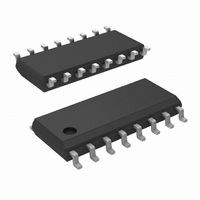
LM3524DMX/NOPB National Semiconductor, LM3524DMX/NOPB Datasheet - Page 14

LM3524DMX/NOPB
Manufacturer Part Number
LM3524DMX/NOPB
Description
IC REG PULSE WIDTH MOD 16-SOIC
Manufacturer
National Semiconductor
Type
Step-Down (Buck), Step-Up (Boost), Flybackr
Datasheet
1.LM2524DNNOPB.pdf
(22 pages)
Specifications of LM3524DMX/NOPB
Internal Switch(s)
Yes
Synchronous Rectifier
No
Number Of Outputs
1
Voltage - Output
5V
Current - Output
200mA
Frequency - Switching
550kHz
Voltage - Input
8 ~ 40 V
Operating Temperature
0°C ~ 125°C
Mounting Type
Surface Mount
Package / Case
16-SOIC (3.9mm Width)
Power - Output
1W
Number Of Pwm Outputs
2
On/off Pin
Yes
Adjustable Output
Yes
Switching Freq
350KHz
Duty Cycle
49%
Operating Supply Voltage (max)
40V
Output Current
200A
Output Voltage
60V
Synchronous Pin
Yes
Rise Time
200ns
Fall Time
100ns
Operating Temperature Classification
Commercial
Mounting
Surface Mount
Pin Count
16
Package Type
SOIC N
Lead Free Status / RoHS Status
Lead free / RoHS Compliant
Other names
*LM3524DMX
*LM3524DMX/NOPB
LM3524DMX
*LM3524DMX/NOPB
LM3524DMX
www.national.com
Also, see LM1578 data sheet for graphical methods of induc-
tor selection.
CALCULATING OUTPUT FILTER CAPACITOR C
Figure 13 shows L1's current with respect to Q1's t
t
to the load and C
between I
From Figure 13 it can be seen that current will be flowing into
C
time, t
The resulting ΔV
For best regulation, the inductor's current cannot be allowed
to fall to zero. Some minimum load current I
ductor current, is required as shown below:
OFF
o
for the second half of t
times (V
ON
/2 + t
L
, and I
A
OFF
is at the collector of Q1). This curent must flow
c
o
/2. The current flowing for this time is ΔI
.
o
or ΔV
. C
o
's current will then be the difference
o
Ic
ON
is described by:
o
= I
through the first half of t
L
− I
o
o
, and thus in-
o
OFF
:
ON
, or a
and
L
/4.
14
A complete step-down switching regulator schematic, using
the LM3524D, is illustrated in Figure 15. Transistors Q1 and
Q2 have been added to boost the output to 1A. The 5V reg-
ulator of the LM3524D has been divided in half to bias the
error amplifier's non-inverting input to within its common-
mode range. Since each output transistor is on for half the
period, actually 45%, they have been paralleled to allow
longer possible duty cycle, up to 90%. This makes a lower
possible input voltage. The output voltage is set by:
where V
input.
Resistor R3 sets the current limit to:
Figures 16, 17 and show a PC board layout and stuffing dia-
gram for the 5V, 1A regulator of Figure 15. The regulator's
performance is listed in Table 1.
FIGURE 14. Inductor Current Slope in Step-Down
NI
is the voltage at the error amplifier's non-inverting
Regulator
865019


