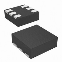
ISL9104IRUBZ-T Intersil, ISL9104IRUBZ-T Datasheet - Page 12

ISL9104IRUBZ-T
Manufacturer Part Number
ISL9104IRUBZ-T
Description
IC CONV SYNC 4.3MHZ 500MA 6-TDFN
Manufacturer
Intersil
Type
Step-Down (Buck)r
Datasheet
1.ISL9104AIRUAZ-T.pdf
(13 pages)
Specifications of ISL9104IRUBZ-T
Internal Switch(s)
Yes
Synchronous Rectifier
Yes
Number Of Outputs
1
Voltage - Output
1.5V
Current - Output
500mA
Frequency - Switching
4.3MHz
Voltage - Input
2.7 ~ 6 V
Operating Temperature
-40°C ~ 85°C
Mounting Type
Surface Mount
Package / Case
6-µTDFN
Lead Free Status / RoHS Status
Lead free / RoHS Compliant
Power - Output
-
Intersil products are sold by description only. Intersil Corporation reserves the right to make changes in circuit design, software and/or specifications at any time without
notice. Accordingly, the reader is cautioned to verify that data sheets are current before placing orders. Information furnished by Intersil is believed to be accurate and
reliable. However, no responsibility is assumed by Intersil or its subsidiaries for its use; nor for any infringements of patents or other rights of third parties which may result
from its use. No license is granted by implication or otherwise under any patent or patent rights of Intersil or its subsidiaries.
VOUT (V)
TABLE 1. RECOMMENDED IISL9104, ISL9104A
0.8
1.0
1.2
1.5
1.8
2.5
2.8
3.3
L (µH)
ADJUSTABLE OUTPUT VERSION CIRCUIT
CONFIGURATION vs V
1.0
1.0
1.0
1.0
1.0
1.0
1.0
1.0
All Intersil U.S. products are manufactured, assembled and tested utilizing ISO9000 quality systems.
Intersil Corporation’s quality certifications can be viewed at www.intersil.com/design/quality
C2 (µF)
For information regarding Intersil Corporation and its products, see www.intersil.com
4.7
4.7
4.7
4.7
4.7
4.7
4.7
4.7
12
R1 (kΩ)
44.2
80.6
84.5
100
100
100
102
OUT
0
C3 (pF)
N/A
100
47
47
47
47
47
47
ISL9104, ISL9104A
R2 (kΩ)
97.6
80.6
47.5
40.2
32.4
N/A
178
162
Layout Recommendation
The PCB layout is a very important converter design step to
make sure the designed converter works well, especially
under the high current high switching frequency condition.
For ISL9104, ISL9104A, the power loop is composed of the
output inductor L, the output capacitor C
the PGND pin. It is necessary to make the power loop as
small as possible and the connecting traces among them
should be direct, short and wide; the same type of traces
should be used to connect the VIN pin, the input capacitor
C
The switching node of the converter, the SW pin, and the
traces connected to this node are very noisy, so keep the
voltage feedback trace and other noise sensitive traces
away from these noisy traces.
The input capacitor should be placed as close as possible to
the VIN pin. The ground of the input and output capacitors
should be connected as close as possible as well. In
addition, a solid ground plane is helpful for EMI performance.
IN
and its ground.
OUT
, the SW pin and
November 24, 2009
FN6829.4


