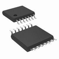
LM3150MH/NOPB National Semiconductor, LM3150MH/NOPB Datasheet - Page 13

LM3150MH/NOPB
Manufacturer Part Number
LM3150MH/NOPB
Description
IC REG SWITCH CTRL 6-42V 14TSSOP
Manufacturer
National Semiconductor
Series
PowerWise®, SIMPLE SWITCHER®r
Type
Step-Down (Buck)r
Datasheet
1.LM3150MHENOPB.pdf
(20 pages)
Specifications of LM3150MH/NOPB
Internal Switch(s)
No
Synchronous Rectifier
Yes
Number Of Outputs
1
Voltage - Output
Adj to 0.6V
Current - Output
12A
Frequency - Switching
1MHz
Voltage - Input
6 ~ 42 V
Operating Temperature
-40°C ~ 125°C
Mounting Type
Surface Mount
Package / Case
14-TSSOP Exposed Pad, 14-eTSSOP 14-HTSSOP
Package
14TSSOP EP
Output Voltage
0.6(Min) V
Output Current
12(Max) A
For Use With
551600142-002 - WEBENCH BUILD IT BOARD LM3150
Lead Free Status / RoHS Status
Lead free / RoHS Compliant
Power - Output
-
Other names
LM3150MH
Available stocks
Company
Part Number
Manufacturer
Quantity
Price
Company:
Part Number:
LM3150MH/NOPB
Manufacturer:
TI
Quantity:
11 235
Part Number:
LM3150MH/NOPB
Manufacturer:
TI/德州仪器
Quantity:
20 000
5. Determine Output Capacitance
Typical hysteretic COT converters similar to the LM3150 re-
quire a certain amount of ripple that is generated across the
ESR of the output capacitor and fed back to the error com-
parator. Emulated Ripple Mode control built into the LM3150
will recreate a similar ripple signal and thus the requirement
for output capacitor ESR will decrease compared to a typical
Hysteretic COT converter. The emulated ripple is generated
by sensing the voltage signal across the low-side FET and is
then compared to the FB voltage at the error comparator input
to determine when to initiate the next on-time period.
The maximum ESR allowed to prevent over-voltage protec-
tion during normal operation is:
ET
A
A
The minimum ESR must meet both of the following criteria:
ET
Any additional parallel capacitors should be chosen so that
their effective impedance will not negatively attenuate the
output ripple voltage.
6. Determine The Use of Feed-Forward Capacitor
Certain applications may require a feed-forward capacitor for
improved stability and easier selection of available output ca-
pacitance. Use the following equation to calculate the value
of C
7. MOSFET and R
The high-side and low-side FETs must have a drain to source
(V
Use the following equations to calculate the desired target
value of the low-side FET R
The gate drive current from VCC must not exceed the mini-
mum current limit of VCC. The drive current from VCC can be
calculated with:
Where, Q
side and low-side FETs.
The plateau voltage of the FET V
Figure
f
f
DS
= V
= 1 if there is a feed-forward capacitor used
min
max
ff
) rating of at least 1.2 x V
I
.
LIM-TH
ESR
OUT
is calculated using V
is calculated using V
4, must be less than VCC - 750 mV.
gtotal
/ 0.6 if there is no feed-forward capacitor used
ESR
ESR
min
Z
(T
FB
C
j
) = I
≥
ff
is the combined total gate charge of the high-
= (R
min
max
[ ET
= V
C
LIM-TH
I
VCCdrive
≥
= (80 mV x L x A
Omin
LIM
FB1
OUT
max
(15 mV x L x A
Selection
x R
/(V
x [1 + 3.3 x 10
= 70 / (f
/ (V
= Q
IN-MIN
FB2
IN-MIN
IN
IN-MAX
DS(ON)
)/(R
gtotal
- V
IN
s
.
x f
2
OUT
FB1
GS
.
x L)
x f
S
for current limit.
f
f
) / ET
x Z
vs Q
) / ET
) ] x (A
S
+ R
-3
FB
x (T
FB2
g
)
max
min
curve, as shown in
f
)
j
/ C
- 27)]
O
)
(17)
(18)
(19)
(20)
(21)
(22)
(23)
(24)
(25)
13
See following design example for estimated power dissipation
calculation.
8. Calculate Input Capacitance
The main parameters for the input capacitor are the voltage
rating, which must be greater than or equal to the maximum
DC input voltage of the power supply, and its rms current rat-
ing. The maximum rms current is approximately 50% of the
maximum load current.
Where, ΔV
age. A good starting point for the input ripple voltage is 5% of
V
When using low ESR ceramic capacitors on the input of the
LM3150 a resonant circuit can be formed with the impedance
of the input power supply and parasitic impedance of long
leads/PCB traces to the LM3150 input capacitors. It is rec-
ommended to use a damping capacitor under these circum-
stances, such as aluminum electrolytic that will prevent
ringing on the input. The damping capacitor should be chosen
to be approximately 5 times greater than the parallel ceramic
capacitors combination. The total input capacitance should
be greater than 10 times the input inductance of the power
supply leads/pcb trace. The damping capacitor should also
be chosen to handle its share of the rms input current which
is shared proportionately with the parallel impedance of the
ceramic capacitors and aluminum electrolytic at the LM3150
switching frequency.
The C
The recommended value is 0.1 µF.
9. Calculate Soft-Start Capacitor
Where t
10. C
C
mended value of 1 µF to 4.7 µF. C
to drive the gate of the high-side FET. It is charged during the
SW off-time. The recommended value for C
IN
VCC
.
FIGURE 4. Typical MOSFET Gate Charge Curve
VCC
should be placed directly at the VCC pin with a recom-
BYP
ss
, C
capacitor should be placed directly at the VIN pin.
is the soft-start time in seconds and V
IN-MAX
BST
and C
is the maximum allowable input ripple volt-
EN
BST
creates a voltage used
BST
is 0.47 µF. The
ref
30053181
www.national.com
= 0.6V.
(26)
(27)


