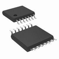
LM3150MH/NOPB National Semiconductor, LM3150MH/NOPB Datasheet - Page 18

LM3150MH/NOPB
Manufacturer Part Number
LM3150MH/NOPB
Description
IC REG SWITCH CTRL 6-42V 14TSSOP
Manufacturer
National Semiconductor
Series
PowerWise®, SIMPLE SWITCHER®r
Type
Step-Down (Buck)r
Datasheet
1.LM3150MHENOPB.pdf
(20 pages)
Specifications of LM3150MH/NOPB
Internal Switch(s)
No
Synchronous Rectifier
Yes
Number Of Outputs
1
Voltage - Output
Adj to 0.6V
Current - Output
12A
Frequency - Switching
1MHz
Voltage - Input
6 ~ 42 V
Operating Temperature
-40°C ~ 125°C
Mounting Type
Surface Mount
Package / Case
14-TSSOP Exposed Pad, 14-eTSSOP 14-HTSSOP
Package
14TSSOP EP
Output Voltage
0.6(Min) V
Output Current
12(Max) A
For Use With
551600142-002 - WEBENCH BUILD IT BOARD LM3150
Lead Free Status / RoHS Status
Lead free / RoHS Compliant
Power - Output
-
Other names
LM3150MH
Available stocks
Company
Part Number
Manufacturer
Quantity
Price
Company:
Part Number:
LM3150MH/NOPB
Manufacturer:
TI
Quantity:
11 235
Part Number:
LM3150MH/NOPB
Manufacturer:
TI/德州仪器
Quantity:
20 000
PCB Layout Considerations
It is good practice to layout the power components first, such
as the input and output capacitors, FETs, and inductor. The
first priority is to make the loop between the input capacitors
and the source of the low-side FET to be very small and tie
the grounds of the low-side FET and input capacitor directly
to each other and then to the ground plane through vias. As
shown in
Figure 6
when the input capacitor ground is tied di-
rectly to the source of the low-side FET, parasitic inductance
in the power path, along with noise coupled into the ground
plane, are reduced.
The switch node is the next item of importance. The switch
node should be made only as large as required to handle the
load current. There are fast voltage transitions occurring in
the switch node at a high frequency, and if the switch node is
made too large it may act as an antennae and couple switch-
ing noise into other parts of the circuit. For high power de-
signs, it is recommended to use a multi-layer board. The FETs
are going to be the largest heat generating devices in the de-
30053158
sign, and as such, care should be taken to remove the heat.
On multi-layer boards using exposed-pad packages for the
FIGURE 6. Schematic of Parasitics
FETs such as the power-pak SO-8, vias should be used under
the FETs to the same plane on the interior layers to help dis-
sipate the heat and cool the FETs. For the typical single FET
Power-Pak type FETs, the high-side FET DAP is V
. The
IN
V
plane should be copied to the other interior layers to the
IN
bottom layer for maximum heat dissipation. Likewise, the
DAP of the low-side FET is connected to the SW node and
the SW node shape should be duplicated to the other PCB
layers for maximum heat dissipation.
See the Evaluation Board application note AN-1900 for an
example of a typical multi-layer board layout, and the Demon-
stration Board Reference Design Application Note for a typi-
cal 2 layer board layout. Each design allows for single sided
30053180
component mounting.
FIGURE 7. PCB Placement of Power Stage
www.national.com
18


