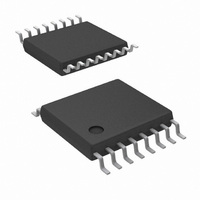
LM2653MTC-ADJ/NOPB National Semiconductor, LM2653MTC-ADJ/NOPB Datasheet - Page 2

LM2653MTC-ADJ/NOPB
Manufacturer Part Number
LM2653MTC-ADJ/NOPB
Description
IC REGULATOR SWITCHING 16-TSSOP
Manufacturer
National Semiconductor
Type
Step-Down (Buck)r
Datasheet
1.LM2653MTCX-ADJNOPB.pdf
(12 pages)
Specifications of LM2653MTC-ADJ/NOPB
Internal Switch(s)
Yes
Synchronous Rectifier
Yes
Number Of Outputs
1
Voltage - Output
1.5 ~ 5 V
Current - Output
1.5A
Frequency - Switching
300kHz
Voltage - Input
4 ~ 14 V
Operating Temperature
-40°C ~ 125°C
Mounting Type
Surface Mount
Package / Case
16-TSSOP
Power - Output
893mW
Msl
MSL 1 - Unlimited
Power Dissipation Pd
893mW
Supply Voltage Range
4V To 14V
Termination Type
SMD
Driver Case Style
TSSOP
No. Of Pins
16
Rohs Compliant
Yes
Filter Terminals
SMD
Input Voltage Primary Max
14V
Leaded Process Compatible
Yes
No. Of Outputs
1
For Use With
LM2653-ADJEVAL - EVALUATION BOARD FOR LM2653-ADJ
Lead Free Status / RoHS Status
Lead free / RoHS Compliant
Other names
*LM2653MTC-ADJ
*LM2653MTC-ADJ/NOPB
LM2653MTC-ADJ
*LM2653MTC-ADJ/NOPB
LM2653MTC-ADJ
Available stocks
Company
Part Number
Manufacturer
Quantity
Price
Company:
Part Number:
LM2653MTC-ADJ/NOPB
Manufacturer:
NS/TI
Quantity:
1 100
www.national.com
V
V
V
V
I
I
V
I
I
R
R
I
CL
SM
Q
QSD
L
FB
OUT
INUV
UV_HYST
HYST
DS(ON)
SW(ON)
Absolute Maximum Ratings
If Military/Aerospace specified devices are required,
please contact the National Semiconductor Sales Office/
Distributors for availability and specifications.
Electrical Characteristics
Specifications with standard typeface are for T
Range. V
Input Voltage
PGOOD Pin Voltage
Feedback Pin Voltage
Power Dissipation (T
Junction Temperature
Storage Temperature Range
Symbol
(Note 2)
Range
IN
= 10V unless otherwise specified.
Feedback Voltage
Output Voltage Line
Regulation
Output Voltage Load
Regulation
Output Voltage Load
Regulation
V
Threshold Voltage
Hysteresis for the Input
Undervoltage Lockout
Switch Current Limit
Sleep Mode Threshold
Current
Sleep Mode Feedback
Voltage Hysteresis
Quiescent Current
Quiescent Current in
Shutdown Mode
High-Side or Low-Side
MOSFET ON Resistance
High-Side or Low-Side
Switch On Resistance
(MOSFET ON Resistance +
Bonding Wire Resitstance)
Switch Leakage
Current — High Side
Switch Leakge
Current — Low Side
IN
Undervoltage Lockout
A
Parameter
=25˚C),
−40˚C ≤ T
−0.4V ≤ V
−65˚C to +150˚C
I
V
I
I
V
I
V
Rising Edge
V
V
V
Shutdown Pin Pulled Low
I
I
LOAD
LOAD
LOAD
LOAD
SWITCH
SWITCH
IN
IN
IN
IN
OUT
IN
J
(Note 1)
= 25˚C, and those in boldface type apply over full Operating Temperature
= 4V to 12V
= 5V
= 5V
= 5V
= 5V, V
J
= 2.5V
= 900 mA
= 900 mA
= 10 mA to 1.5A
= 200 mA to 1.5A
≤ +125˚C
893 mW
FB
= 1A
= 1A
≤ 5V
OUT
15V
15V
Conditions
= 2.5V
2
Operating Ratings
Lead Temperature
M Package
Maximum Junction Temperature
ESD Susceptibility
Supply Voltage
Vapor Phase (60 sec.)
Infrared (15 sec.)
Human Body Model (Note 3)
(Note 5)
Typical
1.238
210
100
110
130
130
0.2
1.3
0.3
3.8
2.0
1.7
24
75
7
(Note 1)
(Note 4)
1.200
1.263
12/20
Limit
3.95
1.55
2.60
130
2.0
4V ≤ V
mΩ (max)
mA(max)
µA(max)
IN
V(max)
V(max)
A(max)
V(min)
A(min)
Units
mΩ
mΩ
mV
mA
mV
mA
≤ 14V
µA
nA
nA
%
%
%
V
V
A
215˚C
220˚C
150˚C
1 kV


