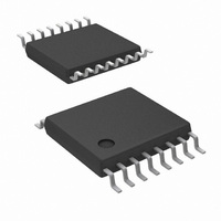
LM2653MTC-ADJ/NOPB National Semiconductor, LM2653MTC-ADJ/NOPB Datasheet - Page 4

LM2653MTC-ADJ/NOPB
Manufacturer Part Number
LM2653MTC-ADJ/NOPB
Description
IC REGULATOR SWITCHING 16-TSSOP
Manufacturer
National Semiconductor
Type
Step-Down (Buck)r
Datasheet
1.LM2653MTCX-ADJNOPB.pdf
(12 pages)
Specifications of LM2653MTC-ADJ/NOPB
Internal Switch(s)
Yes
Synchronous Rectifier
Yes
Number Of Outputs
1
Voltage - Output
1.5 ~ 5 V
Current - Output
1.5A
Frequency - Switching
300kHz
Voltage - Input
4 ~ 14 V
Operating Temperature
-40°C ~ 125°C
Mounting Type
Surface Mount
Package / Case
16-TSSOP
Power - Output
893mW
Msl
MSL 1 - Unlimited
Power Dissipation Pd
893mW
Supply Voltage Range
4V To 14V
Termination Type
SMD
Driver Case Style
TSSOP
No. Of Pins
16
Rohs Compliant
Yes
Filter Terminals
SMD
Input Voltage Primary Max
14V
Leaded Process Compatible
Yes
No. Of Outputs
1
For Use With
LM2653-ADJEVAL - EVALUATION BOARD FOR LM2653-ADJ
Lead Free Status / RoHS Status
Lead free / RoHS Compliant
Other names
*LM2653MTC-ADJ
*LM2653MTC-ADJ/NOPB
LM2653MTC-ADJ
*LM2653MTC-ADJ/NOPB
LM2653MTC-ADJ
Available stocks
Company
Part Number
Manufacturer
Quantity
Price
Company:
Part Number:
LM2653MTC-ADJ/NOPB
Manufacturer:
NS/TI
Quantity:
1 100
www.national.com
Electrical Characteristics
Note 2: The maximum allowable power dissipation is calculated by using P
ambient temperature, and θ
140˚C/W for T
allows the safe dissipation of more power. The Absolute Maximum power dissipation must be derated by 7.14 mW per ˚C above 25˚C ambient. The LM2653 actively
limits its junction temperatures to about 165˚C.
Note 3: The human body model is a 100 pF capacitor discharged through a 1.5 kΩ resistor into each pin.
Note 4: Typical numbers are at 25˚C and represent the most likely norm.
Note 5: All limits guaranteed at room temperature (standard typeface) and at temperature extremes (bold typeface). All room temperature limits are 100%
production tested. All limits at temperature extremes are guaranteed via correlation using standard Statistical Quality Control (SQC) methods. All limits are used
to calculate Average Outgoing Quality Level (AOQL).
Typical Performance Characteristics
JMAX
Frequency vs Junction Temperature
, T
Efficiency vs Load Current
A
, and θ
(V
I
QSD
IN
JA
JA
= 5V, V
vs Input Voltage
is the junction-to-ambient thermal resistance of the specified package. The 893 mW rating results from using 150˚C, 25˚C, and
respectively. A θ
OUT
= 2.5V)
JA
of 140˚C/W represents the worst-case condition of no heat sinking of the 16-pin TSSOP package. Heat sinking
(Continued)
10104925
10104907
10104922
DMAX
4
= (T
JMAX
− T
A
)/θ
JA
, where T
I
QSD
R
SW(ON)
vs Junction Temperature
JMAX
is the maximum junction temperature, T
l
vs Input Voltage
Q
vs V
IN
10104904
10104926
10104923
A
is the


