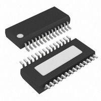
MAX8513EEI+ Maxim Integrated Products, MAX8513EEI+ Datasheet - Page 30

MAX8513EEI+
Manufacturer Part Number
MAX8513EEI+
Description
IC SUPPLY TRPL W/MON 28QSOP
Manufacturer
Maxim Integrated Products
Type
Step-Down (Buck)r
Datasheet
1.MAX8513EEIT.pdf
(35 pages)
Specifications of MAX8513EEI+
Internal Switch(s)
No
Synchronous Rectifier
No
Number Of Outputs
3
Voltage - Output
1.25 ~ 5.5 V
Current - Output
40mA
Frequency - Switching
300kHz ~ 1.4MHz
Voltage - Input
4.5 ~ 28 V
Operating Temperature
-40°C ~ 85°C
Mounting Type
Surface Mount
Package / Case
28-QSOP
Power - Output
860mW
Lead Free Status / RoHS Status
Lead free / RoHS Compliant
Wide-Input, High-Frequency, Triple-Output Supplies
with Voltage Monitor and Power-On Reset
If the second pole occurs well after unity-gain
crossover, the linear regulator remains stable. If not,
then increase the output capacitance C
Typical Applications Circuits) so:
If high-ESR capacitors are used for the output capaci-
tor (C
FB3_. This is accomplished by adding a capacitor
(C
Connect at least a 1µF capacitor between the linear regu-
lator’s output and ground, as close to the MAX8513/
MAX8514 and the external pass transistors as possible.
Depending on the selected pass transistor, larger capaci-
tor values may be required for stability (see the Stability
Requirements section). Once the minimum capacitor
value for stability is determined, verify that the linear regu-
lator’s output does not contain excessive noise. Although
adequate for stability, small capacitor values can provide
too much bandwidth, making the linear regulator sensitive
to noise. Larger capacitor values reduce the bandwidth,
thereby reducing the regulator’s noise sensitivity. For the
negative linear regulator, if noise on the ground reference
causes the design to be marginally stable, bypass the
negative output back to its reference voltage (V
Figure 6). This technique reduces the differential noise on
the output. Ensure the voltage rating of the capacitor
exceeds the output voltage.
The high-impedance base driver is susceptible to system
noise, especially when the linear regulator is lightly
loaded. Capacitively coupled switching noise or induc-
tively coupled EMI on the base drive causes fluctuations
in the base current, which appear as noise on the linear
regulator’s output. To avoid this, keep the base-drive
traces away from the step-down converter and as short
as possible to minimize noise coupling. Resistors in
series with the gate drivers (DH and DL) reduce the LX
switching noise generated by the step-down converter.
Additionally, a bypass capacitor (C
across the base-to-emitter resistor (Figure 7). This bypass
capacitor, in addition to the transistor’s input capaci-
30
FB3_
______________________________________________________________________________________
OUT3
) from FB3_ to GND so:
f
POLE
), then cancel the ESR zero with a pole at
C
FB
3
2
f
POLE
_
=
2
=
Base-Drive Noise Reduction
π
2
(
2
C
OUT3_ Output Capacitors
π
>
BE
×
2
+
C
R
×
Q IN
3
f
||
4
C OUT
1
1
R
_
4
)
×
×
BE
R
IN
3
f
ESR
) can be placed
_
OUT3
||
R
12
(C8 in the
REF3N
,
tance, reduces the frequency of the second pole (f
that could destabilize the linear regulator (see the Stability
Requirements section). Therefore, the stability require-
ments determine the maximum base-to-emitter capaci-
tance (C
In systems where the step-down controller’s output
(OUT1) is not the highest voltage, a transformer can be
used to provide additional post-regulated, high-voltage
outputs. The transformer generates unregulated high-
voltage supplies that power the positive and negative
linear regulators. These unregulated supply voltages
must be high enough to keep the pass transistors from
saturating. For positive output voltages, connect the
transformer as shown in the Typical Applications
Circuits where the minimum turns ratio (n
mined by:
where V
voltage under full load. Since power transfer occurs
when the low-side MOSFET is on (DL = high), the trans-
former cannot support heavy loads with high duty
cycles on V
Under no-load conditions, leakage currents from the
pass transistors supply the output capacitor, even
when the transistor is off. Generally, this is not a prob-
lem since the feedback resistors’ current drains the
excess charge. However, charge can build up on the
output capacitor over temperature, making V
above its set point. Care must be taken to ensure the
feedback resistors’ current exceeds the pass transis-
tor’s leakage current over the entire temperature range.
The power dissipated by the series pass transistor is
calculated by:
where V
the absolute value of the difference between V
V
winding ratio. The transistor must be adequately heat
sunk to prevent a thermal runaway condition. Refer to
the transistor data sheet for thermal calculation.
OUT2/3
BE
Q4(SAT)
IN
is taken. V
) that can be added.
P
is the input to the transistor of the LDO and
n
OUT1
n
D
2
1
≥
=
is OUT3P’s pass transistor’s saturation
.
V
(
Minimum Load Requirements
|
OUT
V
IN
IN
-
3
is derived from the transformer
V
_
OUT
Thermal Consideration
+
Transformer Selection
V
OUT
V
2 3
Q SAT
/
(Linear Regulators)
4
1
|
(
)
×
I
)
OUT
+
V
D
2 3
2
2
/
/n
1
OUT2/3
) is deter-
IN
POLE2
and
rise
)


