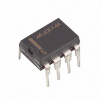
MAX639CPA Maxim Integrated Products, MAX639CPA Datasheet - Page 10

MAX639CPA
Manufacturer Part Number
MAX639CPA
Description
IC DC/DC CONV STEP-DOWN 5V 8-DIP
Manufacturer
Maxim Integrated Products
Type
Step-Down (Buck)r
Datasheet
1.MAX639CPA.pdf
(13 pages)
Specifications of MAX639CPA
Internal Switch(s)
Yes
Synchronous Rectifier
No
Number Of Outputs
1
Voltage - Output
5V, 1.3 ~ 11.5 V
Current - Output
225mA
Voltage - Input
4 ~ 11.5 V
Operating Temperature
0°C ~ 70°C
Mounting Type
Through Hole
Package / Case
8-DIP (0.300", 7.62mm)
Power - Output
727mW
Lead Free Status / RoHS Status
Contains lead / RoHS non-compliant
Frequency - Switching
-
Other names
Q724982
Available stocks
Company
Part Number
Manufacturer
Quantity
Price
Company:
Part Number:
MAX639CPA
Manufacturer:
MAXIM
Quantity:
5 510
Company:
Part Number:
MAX639CPA
Manufacturer:
ROCKWELL
Quantity:
5 510
Company:
Part Number:
MAX639CPA+
Manufacturer:
UMC
Quantity:
6 255
Step 3: L = 50 / I
Step 4: Make sure that I
Inductor series resistance affects both efficiency and
dropout voltage. A high series resistance severely limits
the maximum current available at lower input voltages.
Output currents up to 225mA are possible if the induc-
tor has low series resistance. Inductor and series
switch resistance form an LR circuit during t
L/R time constant is less than the oscillator t
inductor’s peak current will fall short of the desired
I
To maximize efficiency, choose the highest-value
inductor that will provide the required output current
over the whole range of your input voltage (see Typical
Operating Characteristics). Inductors with peak cur-
rents in the 600mA range do not need to be very large.
They are about the size of a 1W resistor, with surface-
mount versions less than 5mm in diameter. Table 1 lists
suppliers of inductors suitable for use with the
MAX639/MAX640/MAX653.
The MAX639/MAX640/MAX653’s output ripple has two
components. One component results from the variation
in stored charge on the filter capacitor with each LX
pulse. The other is the product of the current into the
capacitor and the capacitor’s equivalent series resis-
tance (ESR).
The amount of charge delivered in each oscillator pulse
is determined by the inductor value and input voltage.
5V/3.3V/3V/Adjustable, High-Efficiency,
Low I
Figure 4. Adjustable-Output Operation
10
PEAK
+4.0V TO +11.5V
100µF
C
IN
______________________________________________________________________________________
INPUT
.
8
6
inductor of less than 100µH.
the inductor’s maximum current rating,
whichever is lower.
SHDN
V+
Q
GND
MAX639
MAX640
MAX653
4
, Step-Down DC-DC Converters
PEAK
LBI
3
VOUT
. L will be in µH. Do not use an
VFB 7
PEAK
Output Filter Capacitor
LX
5
1
does not exceed 0.6A or
1N5817
L = 100µH
R3
R4
ON
OUTPUT
ON
. If the
100µF
C
, the
OUT
It decreases with larger inductance, but increases as
the input voltage lessens. As a general rule, a smaller
amount of charge delivered in each pulse results in
less output ripple.
With low-cost aluminum electrolytic capacitors, the
ESR-induced ripple can be larger than that caused by
the charge variation. Consequently, high-quality alu-
minum-electrolytic or tantalum filter capacitors will mini-
mize output ripple. Best results at reasonable cost are
typically achieved with an aluminum-electrolytic capac-
itor in the 100µF range, in parallel with a 0.1µF ceramic
capacitor (Table 1).
In most MAX639/MAX640/MAX653 circuits, the current
in the external diode (D1, Figure 3) changes abruptly
from zero to its peak value each time LX switches off.
To avoid excessive losses, the diode must have a fast
turn-on time. For low-power circuits with peak currents
less than 100mA, signal diodes such as the 1N4148
perform well. The 1N5817 diode works well for high-
power circuits, or for maximum efficiency at low power.
1N5817 equivalent diodes are also available in surface-
mount packages (Table 1). Although the 1N4001 and
other general-purpose rectifiers are rated for high cur-
rents, they are unacceptable because their slow turn-
off times result in excessive losses.
Under no-load conditions, because of leakage from the
PMOS power switch (see the LX Leakage Current vs.
Temperature graph in the Typical Operating
Characteristics) and from the internal resistor from V+
to V
Figure 5. Through-Hole PC Layout and Component Placement
Diagram for Standard Step-Down Application (Top-Side View)
OUT
, leakage current may be supplied to the output
MAX639
MAX640
MAX653
External Diode
Minimum Load


