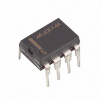
MAX639CPA Maxim Integrated Products, MAX639CPA Datasheet - Page 8

MAX639CPA
Manufacturer Part Number
MAX639CPA
Description
IC DC/DC CONV STEP-DOWN 5V 8-DIP
Manufacturer
Maxim Integrated Products
Type
Step-Down (Buck)r
Datasheet
1.MAX639CPA.pdf
(13 pages)
Specifications of MAX639CPA
Internal Switch(s)
Yes
Synchronous Rectifier
No
Number Of Outputs
1
Voltage - Output
5V, 1.3 ~ 11.5 V
Current - Output
225mA
Voltage - Input
4 ~ 11.5 V
Operating Temperature
0°C ~ 70°C
Mounting Type
Through Hole
Package / Case
8-DIP (0.300", 7.62mm)
Power - Output
727mW
Lead Free Status / RoHS Status
Contains lead / RoHS non-compliant
Frequency - Switching
-
Other names
Q724982
Available stocks
Company
Part Number
Manufacturer
Quantity
Price
Company:
Part Number:
MAX639CPA
Manufacturer:
MAXIM
Quantity:
5 510
Company:
Part Number:
MAX639CPA
Manufacturer:
ROCKWELL
Quantity:
5 510
Company:
Part Number:
MAX639CPA+
Manufacturer:
UMC
Quantity:
6 255
Figure 2 shows what happens to the ideal circuit of
Figure 1 if the switch turns on with a 66% duty cycle and
V+ = 3/2 V
than it falls because the magnitude of the voltage
applied during t
Varying the duty cycle and switching frequency keeps
the peak current constant as input voltage varies. The
MAX639/MAX640/MAX653 control the switch (t
t
These three equations ensure constant peak currents for
a given inductor value, across all input voltages (ignoring
the voltage drop across the diode (D1) and the resistive
losses in the switch and inductor). The variable duty
cycle also ensures that the current through the inductor
discharges to zero at the end of each pulse.
Figure 3 shows the MAX639/MAX640/MAX653 block dia-
gram and a typical connection in which 9V is converted
to 5V (MAX639), 3.3V (MAX640), or 3.0V (MAX653). The
sequence of events in this application is as follows:
5V/3.3V/3V/Adjustable, High-Efficiency,
Low I
Figure 3. Block Diagram
8
OFF
33µF
C
_______________________________________________________________________________________
INPUT, +5.5V TO +11.5V (MAX639),
+3.8V TO +11.5V (MAX640), +3.5V TO +11.5V (MAX653)
) according to the following equations:
IN
Equation (1) t
Equation (2) t
Equation (3) I
R1
R2
OUT
Q
3
2
. The inductor current rises more slowly
ON
, Step-Down DC-DC Converters
LBI
LBO
is less than that applied during t
REFERENCE
BANDGAP
ON
OFF
PEAK
+1.28V
= 50µsV / (V+ - V
≥ 50µsV / V
COMPARATOR
= 50µsV / L
ERROR
LOW-BATTERY
COMPARATOR
SHDN
OUT
DUTY-CYCLE
OSCILLATOR
FREQUENCY
VARIABLE
8
AND
OUT
7
VFB
V+
6
)
ON
OFF
and
.
When the output dips:
(1) The error comparator switches high.
(2) The internal oscillator starts (15µs start-up time)
(3) LX turns on and off according to t
When the output voltage recovers:
(1) The comparator switches low.
(2) LX turns off.
(3) The oscillator shuts down to save power.
For operation at the preset output voltage, connect VFB
to GND; no external resistors are required. For other
output voltages, use an external voltage divider. Set the
output voltage using R3 and R4 as determined by the
following formula:
where R4 is any resistance in the 10kΩ to 1MΩ range (typ-
ically 100kΩ), and the VFB threshold is typically 1.28V.
MODE-SELECT
COMPARATOR
and connects to the gate of the LX output driver.
charging and discharging the inductor, and sup-
plying current to the output (as described above).
R3 = R4 [(V
50mV
GND
4
Fixed or Adjustable Output
OUT
/ VFB Threshold) - 1]
VOUT
LX
1
5
1N5817
L = 100µH
MAX639
MAX640
MAX653
ON
5V, 3.3V OR 3.0V
100µF
C
OUT
and t
AT 100mA
OFF
,


