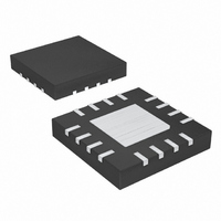
MAX15036ATE+ Maxim Integrated Products, MAX15036ATE+ Datasheet - Page 20

MAX15036ATE+
Manufacturer Part Number
MAX15036ATE+
Description
IC DC/DC CONV 3A 16-TQFN-EP
Manufacturer
Maxim Integrated Products
Type
Step-Down (Buck), Step-Up (Boost)r
Datasheet
1.MAX15036ATEVT.pdf
(25 pages)
Specifications of MAX15036ATE+
Internal Switch(s)
Yes
Synchronous Rectifier
No
Number Of Outputs
1
Voltage - Output
0.6 ~ 28 V
Current - Output
3A
Frequency - Switching
200kHz ~ 2.2MHz
Voltage - Input
4.5 ~ 23 V
Operating Temperature
-40°C ~ 125°C
Mounting Type
Surface Mount
Package / Case
16-TQFN Exposed Pad
Power - Output
2.67W
Lead Free Status / RoHS Status
Lead free / RoHS Compliant
The boost converter compensation gets complicated
due to the presence of a right-half-plane zero f
The right-half-plane zero causes a drop in-phase while
adding positive (+1) slope to the gain curve. It is impor-
tant to drop the gain significantly below unity before the
RHP frequency. Use the following procedure to calculate
the compensation components. (See Figure 4.)
1) Calculate the LC double-pole frequency, f
where:
Target the unity-gain crossover frequency for:
2) Place a zero
where R
3) Calculate C
2.2MHz, 3A Buck or Boost Converters
with an Integrated High-Side Switch
20
the right half plane zero frequency.
______________________________________________________________________________________
F
≥ 10kΩ.
C
A
f
f
C
LC
ZERO RHP
A
=
Boost Converter Compensation
F
for a target crossover frequency, f
V
(
=
=
f
OSC
R
Z
f
C
,
1
2
2
(
MIN
π
π
D
=
≤
⎡
⎣
×
×
= −
2
(
f
)
1
ZERO RHP
1
1
π
0 75
=
=
−
−
.
LC
ω
×
I
D
(
D
OUT MAX
1
V
R
C F IN
5
)
OUT
V
OUT
−
V
,
1
2
1
R V
×
F
IN
OUT
2
D
+
(
f
×
π
LC
)
ω
2
C
×
C
F
R
×
L
2
)
(
)
LC
MIN
R
F
at 0.75 x f
OUT
)
⎤
⎦
ZERO,RHP
LC
LC
, and
C
:
.
.
where ω
4) Place a pole
5) Place the second zero
6) Place the second pole
When using the MAX15036/MAX15037 in noisy environ-
ments, adjust the controller’s compensation to improve
the system’s noise immunity. In particular, high-fre-
quency noise coupled into the feedback loop causes
duty-cycle jitter. One solution is to lower the crossover
frequency (see the Compensation section).
Careful PCB layout is critical to achieve low-switching
power losses and clean stable operation. Use a multi-
layer board whenever possible for better noise immuni-
ty. Follow these guidelines for good PCB layout:
1) Solder the exposed pad to a large copper plane
the switching frequency.
under the IC. To effectively use this copper area as
a heat exchanger between the PCB and the ambi-
ent, expose this copper area on the top and bottom
C
= 2π f
C
CF
R
=
C.
A
(
R
f
P
(
2
=
1
1
π
=
=
2π
×
Improving Noise Immunity
2
2
0 5
×
π
π
.
f
×
×
ZERO
PCB Layout Guidelines
(
×
R
f
(
f
Z
LC
f
1
P
f
A
1
2
SW
2
C
1
×
=
,
×
R
=
F
C
×
HP
2
C
2
A
R
π
A
π
)
F
×
×
×
−
at f
×
C
R
R
1
R
C
1
A
F
1
ZERO,RHP
A
F
×
×
)
C
−
C
1
A
CF
)
at f
)
at 1/2
.
LC
.


