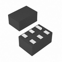
MAX4845ELT+T Maxim Integrated Products, MAX4845ELT+T Datasheet - Page 7

MAX4845ELT+T
Manufacturer Part Number
MAX4845ELT+T
Description
IC CTLR OVP 5.8V 6-UDFN
Manufacturer
Maxim Integrated Products
Type
Overvoltage Protection Controllerr
Datasheet
1.MAX4845ELTT.pdf
(10 pages)
Specifications of MAX4845ELT+T
Applications
Cell Phones, Digital Cameras, Media Players
Mounting Type
Surface Mount
Package / Case
6-µDFN
Lead Free Status / RoHS Status
Lead free / RoHS Compliant
Other names
MAX4845ELT+T
MAX4845ELT+TTR
MAX4845ELT+TTR
The MAX4843–MAX4846 can be used with either a sin-
gle MOSFET configuration as shown in the Typical
Operating Circuit , or can be configured with a back-to-
back MOSFET as shown in Figure 5. The back-to-back
configuration has almost zero reverse current when the
input supply is below the output.
If reverse current leakage is not a concern, a single
MOSFET can be used. This approach has half the loss of
the back-to-back configuration when used with similar
MOSFET types and is a lower cost solution. Note that if
the input is actually pulled low, the output is also pulled
low due to the parasitic body diode in the MOSFET. If
this is a concern, the back-to-back configuration should
be used.
In a typical application of the MAX4846, an external
adapter with built-in battery charger is connected to IN
and a battery is connected to the source of the external
FET. When the adapter is unplugged, IN is directly con-
nected to the battery through the external FET. Since
the battery voltage is typically greater than 3V, the
GATE voltage stays high and the device remains pow-
ered by the battery.
The MAX4843–MAX4846 are designed for use with
either a single n-channel MOSFET or dual back-to-back
n-channel MOSFETs. In most situations, MOSFETs with
R
supply is near the UVLO maximum of 3.5V, consider
using a MOSFET specified for a lower V
Also the V
stand the full 28V IN range of the MAX4843–MAX4846.
Table 1 shows a selection of MOSFETs appropriate for
use with the MAX4843–MAX4846.
Table 1. MOSFET Suggestions
ON
FDC6561AN
FDC6305N
specified for a V
Si5902DC
Si1426DH
PART
DS
should be 30V for the MOSFET to with-
Applications Information
_______________________________________________________________________________________
Overvoltage Protection Controllers with
GS
CONFIGURATION/
Single/SSOT-6
Dual/SSOT-6
Dual/SSOT-6
Dual/1206-8
of 4.5V work well. If the input
PACKAGE
MOSFET Configuration
MOSFET Selection
GS
V
voltage.
DS
MAX (V)
30
30
30
20
For most applications, bypass IN to GND with a 1µF
ceramic capacitor. If the power source has significant
inductance due to long lead length, take care to pre-
vent overshoots due to the LC tank circuit and provide
protection if necessary to prevent exceeding the 30V
absolute maximum rating on IN.
The MAX4843–MAX4846 provide protection against
voltage faults up to 28V, but this does not include nega-
tive voltages. If negative voltages are a concern, con-
nect a Schottky diode from IN to GND to clamp
negative input voltages.
ESD performance depends on a number of conditions.
The MAX4843–MAX4846 are protected from ±15kV typ-
ical ESD on IN when IN is bypassed to ground with a
1µF ceramic capacitor.
Figure 5. Back-to-Back External MOSFET Configuration
INPUT
+1.2V TO +28V
Low Standby Current
1μF
R
ON
at 4.5V (m )
143
115
145
80
2
1
GND
IN
MAX4843–
MAX4846
IN Bypass Considerations
Vishay Siliconix
www.vishay.com
Fairchild Semiconductor
www.fairchildsemi.com
GATE
FLAG
ESD Test Conditions
4
3
MANUFACTURER
N
V
IO
N
7


