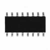
LX5261CDP Microsemi Analog Mixed Signal Group, LX5261CDP Datasheet - Page 3

LX5261CDP
Manufacturer Part Number
LX5261CDP
Description
IC REG SCSI 27LINE LVD 16SOIC
Manufacturer
Microsemi Analog Mixed Signal Group
Datasheet
1.LX5261CDP.pdf
(6 pages)
Specifications of LX5261CDP
Applications
*
Mounting Type
Surface Mount
Package / Case
16-SOIC (3.9mm Width)
Lead Free Status / RoHS Status
Contains lead / RoHS non-compliant
Copyright © 2000
Rev. 1.0c, 2005-02-08
Unless otherwise specified, the following specifications apply over the operating ambient temperature 0°C
3.3V.
VTERM
Signal Line Voltage
Operating Junction Temperature
TERMPWR Section
VTERM Supply Current
VTERM Voltage
Regulator Section
1.75V Regulator
1.3V Regulator
0.75V Regulator
1.75V Regulator Source Current
1.75V Regulator Sink Current
1.75V Source Current Limit
1.75V Sink Current Limit
1.3V Regulator Source Current
1.3V Regulator Sink Current
0.75V Regulator Source Current
0.75V Regulator Sink Current
0.75V Source Current Limit
0.75V Sink Current Limit
TM
Parameter
11861 Western Avenue, Garden Grove, CA. 92841, 714-898-8121, Fax: 714-893-2570
Parameter
R E C O M M E N D E D M A X O P E R A T I N G C O N D I T I O N S
Symbol
E L E C T R I C A L C H A R A C T E R I S T I C S
I
I
DIFS_SRC
DIFS_SNK
V
V
V
I
V
I
I
I
I
TERM
SRC1
SNK1
SRC2
SNK2
TERM
REG1
REG2
DIFS
No Load
-125mA < I
DIFSENS; No Load
-125mA < I
V
V
DIFSENS; 0V
DIFSENS = 2.4V
V
V
Integrated Products Division
OUT
OUT
OUT
OUT
= 1.25V
= 2.25V
= 0.25V
= 1.25V
®
Microsemi
OUT
OUT
< 125mA, 2.7V < V
< 125mA, 2.7V < V
Test Conditions
27-Line LVD SCSI Source/Sink Regulator
Symbol
V
TERM
T
J
IN
IN
P
RODUCTION
< 5.25V
< 5.25V
Min
2.7
0
0
LX5261
D
Typ
ATA
Min
-700
-700
200
200
≤
2.7
1.7
1.2
0.7
50
-5
T
S
A
HEET
≤
LX5261
Typ
1.75
0.75
70°C, and V
1.3
35
Max
5.25
5.0
70
Max
5.25
-200
-200
700
200
700
1.8
1.4
0.8
-15
40
LX5261
TERM
Units
°C
V
V
Units
=
mA
mA
mA
mA
mA
mA
mA
mA
mA
mA
µA
V
V
V
V
Page 3


