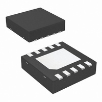
LM8342SD/NOPB National Semiconductor, LM8342SD/NOPB Datasheet - Page 11

LM8342SD/NOPB
Manufacturer Part Number
LM8342SD/NOPB
Description
IC PROG TFT CALIBRATOR 10-LLP
Manufacturer
National Semiconductor
Datasheet
1.LM8342SDXNOPB.pdf
(16 pages)
Specifications of LM8342SD/NOPB
Applications
*
Mounting Type
Surface Mount
Package / Case
10-LLP
Lead Free Status / RoHS Status
Lead free / RoHS Compliant
Other names
LM8342SD
LM8342SDTR
LM8342SDTR
The timing diagram shows the major aspect of the communi-
cation protocol and represents a typical data stream. In case
a master wants to setup a data transfer, it tests if “the bus is
busy.” If it is not busy, then the master starts the data transfer
by creating a “start data transfer” situation. Accordingly the
corresponding receiver is selected by sending the appropriate
“slave address.” This receiver gives an “acknowledge” on
recognizing its address on the bus. The master continues the
data transfer by sending the data stream. Again the receiver
gives an “acknowledge” after receipt. Depending on the
amount of data the master will continue or create a “stop data
transfer” situation. Table 2 gives a more detailed description
of the I
Bus not busy
Start Data Transfer
Slave address
R/W-bit
TABLE 2. Detailed Description of I
2
C compatible communication.
Communication Definitions
The I
when both data (SDA) and clock
(SCL) lines remain HIGH. The
controller can initiate data transfer
only when the bus is not busy.
Starting from an idle state (bus not
busy) a START condition consists of
a HIGH to LOW transition of SDA
while SCL is HIGH. All commands
must start with a START condition.
After generating a start condition, the
master transmits a 7-bit slave
address. (The LM8342 uses the 8th
bit for selecting the R/W operation,
but this does not affect the address.)
The address for the LM8342 is
9E
If the value of the R/W bit is HIGH, the
data is read from the register of the
LM8342. Otherwise the current DAC
setting is written to the LM8342.
HEX
2
C compatible bus is not busy
.
2
C compatible
FIGURE 6. Timing Diagram
11
Acknowledge
Data byte
P-bit
Stop Data Transfer
A receive device, when addressed, is
obliged to generate an “acknowledge”
after the reception of each byte. The
master generates an extra clock cycle
that is associated with this
acknowledge bit. The receiver has to
pull down the SDA line during the
acknowledge clock pulse so that the
SDA line is stable LOW during the
HIGH period of SCL, with respect to
the SCL timing specifications.
A data byte consists of 8 bits. 7 bits
are used for the DAC setting of the
LM8342. The 8th bit is known as the
P-bit.
The function of the P-bit depends on
the Read/Write operation (R/W-bit).
During a Read operation of the
LM8342, the P-bit indicates the
programming state of the EEPROM.
During a Write operation, the register
or both the register and the EEPROM
of the LM8342 can be selected as
destination. A more detailed
description of the P-bit is given in
Table 3 .
A STOP condition consists of a LOW
to HIGH transition of SDA while SCL
is HIGH. All operations must be
ended with a STOP condition.
www.national.com
20139204


