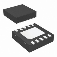
LM8342SD/NOPB National Semiconductor, LM8342SD/NOPB Datasheet - Page 14

LM8342SD/NOPB
Manufacturer Part Number
LM8342SD/NOPB
Description
IC PROG TFT CALIBRATOR 10-LLP
Manufacturer
National Semiconductor
Datasheet
1.LM8342SDXNOPB.pdf
(16 pages)
Specifications of LM8342SD/NOPB
Applications
*
Mounting Type
Surface Mount
Package / Case
10-LLP
Lead Free Status / RoHS Status
Lead free / RoHS Compliant
Other names
LM8342SD
LM8342SDTR
LM8342SDTR
www.national.com
EVALUATION SYSTEM
For the LM8342 a complete evaluation system is available,
including two boards. Figure 10 gives a schematic represen-
tation.
•
•
TABLE 4. Overview Resistor Values for Different R
ΔV
LM8342 Evaluation Board
This board demonstrates the functionality of the LM8342
using the I
LM8342 can easily be demonstrated in 2 applications:
— Programmable current sink
— Programmable V
LM8342 Programmer Board
This test board has dedicated functionality for
communicating with the LM8342, using the I
interface. This board can operate in two different modes:
— Write mode: The digitized value of a potentiometer
— Read mode: The board reads the stored values from
±0.5
±1.5
±2.5
(V)
±1
±2
±3
COM
setting is written to the LM8342. The user can select
on the programmer board to write the data to the
register or to store the data in the EEPROM.
the LM8342’s EEPROM and presents this data onto a
3-digit display.
R
FIGURE 10. LM8342 Evaluation System
SET
AV
2
47.1k
66.7k
84.2k
100k
114k
= 10 kΩ
C compatible interface for communication. The
25k
(Ω)
R1
DD
Settings at AV
= 15V (V
28.6k
61.5k
COM
100k
146k
200k
267k
(Ω)
R2
level driver
COM
Level = 7.5 V)
DD
ΔV
±0.5
±1.5
±2.5
(V)
±1
±2
±3
= 15V
COM
R
SET
= 45 kΩ
113k
212k
300k
379k
450k
514k
(Ω)
R1
2
C compatible
1.2M
129k
277k
450k
655k
900k
(Ω)
20139232
R2
SET
14
LAYOUT RECOMMENDATIONS
A proper layout is necessary for optimum performance of the
LM8342. A low impedance and proper ground plane (free of
disturbances) is recommended, since a current of up to 10
mA can flow with HF contents during programming. The
traces from the GND pin to the ground plane should be as
short as possible. It is recommended to place decoupling ca-
pacitors close to the V
decoupling capacitors to the ground plane should be short.
As SET is a sensitive input, crosstalk to that pin should be
prevented. Special care should be taken when routing the in-
terface connections. The signals on the serial interface can
be more than 60 dB larger than the equivalent LSB at the SET
input pin. Crosstalk between the interface bus and R
sults in disturbance of the output current I
For applications requiring a low output current (using high
values for R
attention should be paid to the parasitic capacitance (C
parallel to R
(<1 LSB) unwanted ripple at the output current might be ob-
tained. It is recommended to place the R
the LM8342, in combination with a good board layout to re-
duce this parasitic capacitance.
SET
SET
in combination with low DAC settings) special
. For C
DD
PAR
and AV
larger than tens of pF, a small
DD
pins. Connections of these
SET
OUT
resistor close to
of the LM8342.
SET
PAR
re-
)


