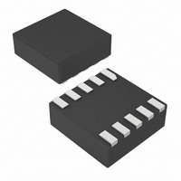
MAX4960ELB+T Maxim Integrated Products, MAX4960ELB+T Datasheet - Page 3

MAX4960ELB+T
Manufacturer Part Number
MAX4960ELB+T
Description
IC CTLR HI VOLTAGE OVP 10-UDFN
Manufacturer
Maxim Integrated Products
Datasheet
1.MAX4959ELBT.pdf
(17 pages)
Specifications of MAX4960ELB+T
Applications
*
Mounting Type
Surface Mount
Package / Case
10-µDFN
Lead Free Status / RoHS Status
Lead free / RoHS Compliant
ELECTRICAL CHARACTERISTICS (continued)
(V
(V
Note 1: Operation is tested at T
Note 2: Do not exceed absolute maximum rating; the ratio between the externally set OVLO and UVLO threshold must not exceed 4,
Note 3: Assertion delay starts from switching of CB pin to reaching of 80% of GATE1/GATE2 transition. This delay is measured without
GATE1 Leakage Current
GATE2 Leakage Current
CB
Logic-Level High
Logic-Level Low
CB Pulldown Resistor
TIMING
Debounce Time
GATE1 Assertion Delay from
CB Pin
GATE2 Assertion Delay from
CB Pin
Blanking Time
MAX4960
SOURCE1/GATE1 Resistance
GATE1/Ground Resistance
OVLO
IN
= +19V, T
12
10
-2
8
6
4
2
0
-150
= 22.2V and V
is tested for µMAX package.
[OVLO/UVLO]
external capacitive load.
PARAMETER
-100
High-Voltage OVP with Battery Switchover
V
A
POWER-UP RESPONSE
GATE1
V
DD
V
= -40°C to +85°C, unless otherwise noted, C
IN
(R
-50
PULLUP
_______________________________________________________________________________________
TIME ( s)
UVLO
MAX
0
= 1k )
≤ 4.
= 10.1V, R1 = 887kΩ, R2 = 66.5kΩ, R3 = 54.9kΩ, all resistors 1%, OV
50
A
= +25
100
SYMBOL
G1I
G2I
t
R
t1
t2
°
BLANK
C and guaranteed by design for µDFN package. Operation over specified temperature range
150
t
R
R
CBPD
V
DEB
GATE
GATE
V
GG
SG
IH
LKG
LKG
IL
V
V
V
GATE1 to go low
CB = +3V to 0
rise time = fall time = 5ns (Note 3)
CB = 0 to +3V
rise time = fall time = 5ns (Note 3)
(MAX4960)
GATE1 Asserted (MAX4960)
30
25
20
15
10
5
0
OV S
CB
OVP
-150
= 0V
> OV
> V
-100
OVERVOLTAGE RESPONSE
IN
V
R E F
GATE1
V
VDD
> V
IN
(R
-50
, V
PULLUP
CONDITIONS
UVP
= 100nF. Typical values are at T
U V S
TIME ( s)
for greater than t
0
< U V
= 5k )
Typical Operating Characteristics
50
R E F
V
DD
, or V
100
C B
150
DEB
= + 5V
for
16
14
12
10
8
6
4
2
0
REF
A
MIN
140
140
0
1.5
10
10
-1
-1
1
V
V
= +25°C.) (Note 1)
IN
GATE1
= UV
10
UNDERVOLTAGE RESPONSE
(WITHIN BLANKING TIME)
REF
TYP
20
200
200
(R
25
50
50
25
2
PULLUP
= 1.228V.)
DRAIN OF P1
TIME ( s)
30
= 1k )
MAX
40
260
260
0.4
+1
+1
40
40
3
50
UNITS
60
MΩ
ms
ms
µA
µA
kΩ
kΩ
ns
ns
V
V
70
3


