NBSG16VSBAHTBG ON Semiconductor, NBSG16VSBAHTBG Datasheet - Page 8
NBSG16VSBAHTBG
Manufacturer Part Number
NBSG16VSBAHTBG
Description
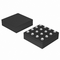
IC RX/DRIVER SIGE DIFF 16-BGA
Manufacturer
ON Semiconductor
Type
Transceiverr
Datasheet
1.NBSG16VSMNR2G.pdf
(14 pages)
Specifications of NBSG16VSBAHTBG
Applications
Instrumentation
Mounting Type
Surface Mount
Package / Case
16-FCBGA
Lead Free Status / RoHS Status
Lead free / RoHS Compliant
Available stocks
Company
Part Number
Manufacturer
Quantity
Price
Company:

Part Number:
NBSG16VSBAHTBG
Manufacturer:
ON Semiconductor
Quantity:
10 000


NOTE: Device will meet the specifications after thermal equilibrium has been established when mounted in a test socket or printed circuit
26. Measured using a 500 mV source, 50% duty cycle clock source. All loading with 50 W to V
27. t
28. V
29. Conditions include input amplitude of 500 mV and V
NOTE: Device will meet the specifications after thermal equilibrium has been established when mounted in a test socket or printed circuit
30. Measured using a 500 mV source, 50% duty cycle clock source. All loading with 50 W to V
31. t
32. V
33. Conditions include input amplitude of 500 mV and V
Table 8. AC CHARACTERISTICS for FCBGA−16
Table 9. AC CHARACTERISTICS for FCBGA−16
Symbol
Symbol
f
t
t
t
t
V
t
t
f
t
t
t
t
V
t
t
max
PLH
PHL
SKEW
JITTER
r
f
max
PLH
PHL
SKEW
JITTER
r
f
INPP
INPP
Spec in Figure 8).
Spec in Figure 9).
SKEW
SKEW
INPP(MAX)
INPP(MAX)
,
,
board with maintained transverse airflow greater than 500 lfpm. Electrical parameters are guaranteed only over the declared
operating temperature range. Functional operation of the device exceeding these conditions is not implied. Device specification limit
values are applied individually under normal operating conditions and not valid simultaneously.
= |t
= |t
Maximum Frequency
(See Figure 8) (Note 26)
Propagation Delay to Output Differen-
tial
Duty Cycle Skew (Note 27)
RMS Random Clock Jitter
Peak−to−Peak Data Dependent Jitter
Input Voltage Swing/Sensitivity
(Differential Configuration) (Note 28)
Output Rise/Fall Times (20% − 80%)
@ 1 GHz
Maximum Frequency
(See Figure 9) (Note 30)
Propagation Delay to Output Differen-
tial
Duty Cycle Skew (Note 31)
RMS Random Clock Jitter
Peak−to−Peak Data Dependent Jitter
Input Voltage Swing/Sensitivity
(Differential Configuration) (Note 32)
Output Rise/Fall Times (20% − 80%)
@ 1 GHz
PLH
PLH
cannot exceed V
cannot exceed V
(V
(V
(V
(V
(V
(V
(V
(V
−t
−t
CTRL
CTRL
CTRL
CTRL
CTRL
CTRL
CTRL
CTRL
PHL
PHL
| for a nominal 50% differential clock input waveform. See Figure 10.
| for a nominal 50% differential clock input waveform. See Figure 10.
= V
= V
= V
= V
= V
= V
= V
= V
Characteristic
Characteristic
CC
CC
CC
CC
CC
CC
CC
CC
− 2 V) D → Q, Q
− 1 V) D → Q, Q
− 2 V) Q, Q
− 1 V) Q, Q
− 2 V) D → Q, Q
− 1 V) D → Q, Q
− 2 V) Q, Q
− 1 V) Q, Q
CC
CC
− V
− V
f
EE
f
EE
in
f
in
f
in
in
< 10 Gb/s
< 10 GHz
(applicable only when V
(applicable only when V
< 10 Gb/s
< 10 GHz
(Note 33)
(Note 29)
CTRL
CTRL
10.7
Min
100
100
10.7
75
25
22
Min
100
100
75
30
30
V
V
http://onsemi.com
CC
CC
= V
= V
−40°C
−40°C
= 0 V; V
= 0 V; −3.0 V tV
CC
CC
CC
CC
TBD
Typ
125
120
TBD
0.9
Typ
125
120
12
50
45
0.8
12
45
40
3
− 2 V. Minimum output amplitude guarantee of 100 mV (see Output P−P
− 2 V. Minimum output amplitude guarantee of 100 mV (see Output P−P
3
− V
− V
8
EE
EE
EE
2600
2600
Max
145
140
Max
145
140
10
70
60
= −3.465 V to −3.0 V or V
10
55
50
3
2
t 2600 mV).
t 2600 mV).
(Note 33)
(Note 29)
EE
10.7
Min
10.7
100
100
Min
100
100
v −2.375 V or 2.375 V v V
75
25
22
75
30
30
25°C
25°C
TBD
TBD
Typ
CC
125
120
CC
Typ
125
120
0.9
12
50
45
0.8
12
45
40
3
3
−2.0 V. Input edge rates 40 ps (20% − 80%).
−2.0 V. Input edge rates 40 ps (20% − 80%).
2600
2600
Max
Max
145
140
145
140
10
70
60
CC
10
55
50
3
2
= 3.0 V to 3.465 V; V
(Note 33)
(Note 29)
10.7
10.7
Min
100
100
Min
100
100
75
25
22
75
30
30
CC
t 3.0 V; V
85°C
85°C
TBD
TBD
Typ
125
120
Typ
125
120
0.9
0.8
12
50
45
12
45
40
3
3
EE
2600
2600
Max
Max
145
140
145
140
EE
10
70
60
10
55
50
3
2
= 0 V
= 0 V
GHz
Unit
GHz
Unit
mV
mV
ps
ps
ps
ps
ps
ps
ps
ps
Related parts for NBSG16VSBAHTBG
Image
Part Number
Description
Manufacturer
Datasheet
Request
R

Part Number:
Description:
2.5v/3.3v Sige Differential Receiver/driver With Variable Output Swing
Manufacturer:
ON Semiconductor
Datasheet:
Part Number:
Description:
ON Semiconductor [VOLTAGE REGULATOR]
Manufacturer:
ON Semiconductor
Datasheet:
Part Number:
Description:
357-036-542-201 CARDEDGE 36POS DL .156 BLK LOPRO
Manufacturer:
ON Semiconductor
Datasheet:
Part Number:
Description:
357-036-542-201 CARDEDGE 36POS DL .156 BLK LOPRO
Manufacturer:
ON Semiconductor
Datasheet:
Part Number:
Description:
357-036-542-201 CARDEDGE 36POS DL .156 BLK LOPRO
Manufacturer:
ON Semiconductor
Datasheet:
Part Number:
Description:
357-036-542-201 CARDEDGE 36POS DL .156 BLK LOPRO
Manufacturer:
ON Semiconductor
Datasheet:
Part Number:
Description:
357-036-542-201 CARDEDGE 36POS DL .156 BLK LOPRO
Manufacturer:
ON Semiconductor
Datasheet:
Part Number:
Description:
357-036-542-201 CARDEDGE 36POS DL .156 BLK LOPRO
Manufacturer:
ON Semiconductor
Datasheet:
Part Number:
Description:
357-036-542-201 CARDEDGE 36POS DL .156 BLK LOPRO
Manufacturer:
ON Semiconductor
Datasheet:
Part Number:
Description:
357-036-542-201 CARDEDGE 36POS DL .156 BLK LOPRO
Manufacturer:
ON Semiconductor
Datasheet:
Part Number:
Description:
357-036-542-201 CARDEDGE 36POS DL .156 BLK LOPRO
Manufacturer:
ON Semiconductor
Datasheet:
Part Number:
Description:
357-036-542-201 CARDEDGE 36POS DL .156 BLK LOPRO
Manufacturer:
ON Semiconductor
Datasheet:
Part Number:
Description:
Manufacturer:
ON Semiconductor
Datasheet: