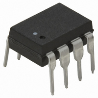
HCPL-3180-000E Avago Technologies US Inc., HCPL-3180-000E Datasheet - Page 15

HCPL-3180-000E
Manufacturer Part Number
HCPL-3180-000E
Description
OPTOCOUPLER 2.0A 250KHZ 8-DIP
Manufacturer
Avago Technologies US Inc.
Datasheet
1.HCPL-3180-000E.pdf
(16 pages)
Specifications of HCPL-3180-000E
Package / Case
8-DIP (0.300", 7.62mm)
Voltage - Isolation
3750Vrms
Number Of Channels
1, Unidirectional
Current - Output / Channel
2.5A
Propagation Delay High - Low @ If
150ns @ 10mA
Current - Dc Forward (if)
16mA
Input Type
DC
Output Type
Gate Driver
Mounting Type
Through Hole
Isolation Voltage
3750 Vrms
Maximum Fall Time
0.025 us
Maximum Forward Diode Current
25 mA
Minimum Forward Diode Voltage
1.2 V
Output Device
Integrated Photo IC
Configuration
1 Channel
Maximum Forward Diode Voltage
1.8 V
Maximum Reverse Diode Voltage
5 V
Maximum Power Dissipation
295 mW
Maximum Operating Temperature
+ 100 C
Minimum Operating Temperature
- 40 C
Number Of Elements
1
Forward Voltage
1.8V
Forward Current
25mA
Package Type
PDIP
Operating Temp Range
-40C to 100C
Power Dissipation
295mW
Propagation Delay Time
200ns
Pin Count
8
Mounting
Through Hole
Reverse Breakdown Voltage
5V
Operating Temperature Classification
Industrial
No. Of Channels
1
Optocoupler Output Type
Gate Drive
Input Current
16mA
Output Voltage
20V
Opto Case Style
DIP
No. Of Pins
8
Common Mode Ratio
10 KV/uS
Rohs Compliant
Yes
Lead Free Status / RoHS Status
Lead free / RoHS Compliant
Lead Free Status / RoHS Status
Lead free / RoHS Compliant, Lead free / RoHS Compliant
Other names
516-1674-5
Available stocks
Company
Part Number
Manufacturer
Quantity
Price
Company:
Part Number:
HCPL-3180-000E
Manufacturer:
AVAGO
Quantity:
6 236
Part Number:
HCPL-3180-000E
Manufacturer:
AVAGO/安华高
Quantity:
20 000
Figure 31. Not recommended open collector drive circuit.
Under Voltage Lockout Feature
The HCPL-3180 contains an under voltage lockout (UVLO)
feature that is designed to protect the IGBT under fault
conditions which cause the HCPL-3180 supply voltage
(equivalent to the fully charged IGBT gate voltage) to
drop below a level necessary to keep the IGBT in a low
resistance state. When the HCPL-3180 output is in the
high state and the supply voltage drops below the HCPL-
3180 V
will go into the low state. When the HCPL-3180 output is
in the low state and the supply voltage rises above the
HCPL-3180 V
output will go into the high state (assume LED is “ON”).
Figure 33. Under voltage lock out.
+5 V
Q1
20
18
16
14
12
10
8
6
4
2
0
0
UVLO-
(V
CC
1
2
3
4
- V
threshold (typ 7.5 V) the optocoupler output
5
UVLO+
EE
) – SUPPLY VOLTAGE – V
C
C
I
LEDN
LEDP
LEDN
SHIELD
threshold (typ 8.5 V) the optocoupler
10
15
20
8
7
6
5
IPM Dead Time and Propagation Delay Specifications
The HCPL-3180 includes a Propagation Delay Difference
(PDD) specification intended to help designers minimize
“dead time” in their power inverter designs. Dead time is
the time during which the high and low side power tran-
sistors are off. Any overlap in Q1 and Q2 conduction will
result in large currents flowing through the power devices
from the high voltage to the low-voltage motor rails.
To minimize dead time in a given design, the turn on of
LED2 should be delayed (relative to the turn off of LED1)
so that under worst-case conditions, transistor Q1 has
just turned off when transistor Q2 turns on, as shown in
Figure 34. The amount of delay necessary to achieve this
condition is equal to the maximum value of the propa-
gation delay difference specification, PDD
specified to be 90 ns over the operating temperature
range of -40 °C to +100 °C.
Figure 32. Recommended LED drive circuit for ultra-high CMR.
V
V
Figure 34. Minimum LED skew for zero dead time.
*PDD = PROPAGATION DELAY DIFFERENCE
NOTE: FOR PDD CALCULATIONS, THE PROPAGATION DELAYS
I
I
OUT1
OUT2
LED1
LED2
+5 V
ARE TAKEN AT THE SAME TEMPERATURE AND TEST CONDITIONS.
1
2
3
4
C
C
LEDP
LEDN
SHIELD
PDD* MAX = (t
t
PHL MAX
Q2 OFF
Q1 ON
PHL
t
PLH MIN
- t
PLH
8
7
6
5
)
MAX
= t
PHL MAX
Q1 OFF
Q2 ON
MAX
- t
, which is
PLH MIN


