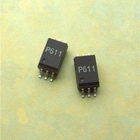
ACPL-P611-560E Avago Technologies US Inc., ACPL-P611-560E Datasheet - Page 8

ACPL-P611-560E
Manufacturer Part Number
ACPL-P611-560E
Description
OPTOCOUPLER 10MBD TTL VDE 6-SOIC
Manufacturer
Avago Technologies US Inc.
Datasheet
1.ACPL-W611-500E.pdf
(11 pages)
Specifications of ACPL-P611-560E
Package / Case
6-SOP
Voltage - Isolation
3750Vrms
Number Of Channels
1, Unidirectional
Current - Output / Channel
50mA
Data Rate
10MBd
Propagation Delay High - Low @ If
50ns @ 7.5mA
Current - Dc Forward (if)
20mA
Input Type
DC
Output Type
Open Collector
Mounting Type
Surface Mount
Isolation Voltage
3750 Vrms
Maximum Continuous Output Current
50 mA
Maximum Fall Time
10 ns
Maximum Forward Diode Current
20 mA
Maximum Rise Time
24 ns
Minimum Forward Diode Voltage
1.4 V
Output Device
Logic Gate Photo IC
Configuration
1 Channel
Maximum Baud Rate
10 MBps
Maximum Forward Diode Voltage
1.75 V
Maximum Reverse Diode Voltage
5 V
Maximum Power Dissipation
85 mW
Maximum Operating Temperature
+ 85 C
Minimum Operating Temperature
- 40 C
Lead Free Status / RoHS Status
Lead free / RoHS Compliant
Switching Specifications (AC)
Over recommended operating conditions T
All typicals at V
Parameter
Propagation Delay Time to
High Output Level
Propagation Delay Time to
Low Output Level
Pulse Width Distortion
Propagation Delay Skew
Output Rise Time (10%-90%)
Output Fall Time (10%-90%)
Output High Level Common
Mode Transient Immunity
Output Low Level Common
Mode Transient Immunity
Package Characteristics
All typicals at T
Parameter
Input-Output Insulation
Input-Output Resistance
Input-Output Capacitance
Notes:
10. See application section; “Propagation Delay, Pulse-Width Distortion and Propagation Delay Skew” for more information.
11. t
8
1. Bypassing of the power supply line is required with a 0.1 μF ceramic disc capacitor adjacent to each optocoupler. The total lead length be-
2. Peaking circuits may produce transient input currents up to 50 mA, 50 ns maximum pulse width, provided average current does not
3. Device considered a two terminal device: pins 1, 2 and 3 shorted together, and pins 4, 5 and 6 shorted together.
4. In accordance with UL 1577, each optocoupler is proof tested by applying an insulation test voltage ≥ 4500 V
5. The t
6. The t
7. CM
8. CM
9. For sinusoidal voltages, (|dV
tween both ends of the capacitor and the isolator pins should not exceed 10 mm.
exceed 20 mA.
tection current limit, I
output pulse.
output pulse.
(i.e., V
(i.e., V
operating condition range.
PSK
H
L
is equal to the worst case differ ence in t
is the maximum tolerable rate of fall of the common mode voltage to assure that the output will remain in a low logic state
is the maximum tolerable rate of rise of the common mode voltage to assure that the output will remain in a high logic state
PLH
PHL
OUT
OUT
propagation delay is measured from 3.75 mA point on the falling edge of the input pulse to the 1.5 V point on the rising edge of the
propagation delay is measured from 3.75 mA point on the rising edge of the input pulse to the 1.5 V point on the falling edge of the
> 2.0 V).
> 0.8 V).
A
CC
= 25 °C.
= 5 V, T
I-O
≤ 5 μA).
A
= 25 °C.
CM
|/dt)
Symbol
t
t
|t
t
t
t
|CM
|CM
Symbol
V
R
C
max
PLH
PHL
PSK
R
F
ISO
I-O
PHL
I-O
= Sf
H
L
- t
|
|
PLH
CM
PHL
|
V
CM(p-p)
and/or t
Min.
20
25
10
10
Min.
3750
A
.
= -40°C to 85°C, V
PLH
that will be seen between units at any given temperature within the worst case
Typ.
48
50
3.5
24
10
15
15
Typ.
10
0.6
12
Max.
75
100
75
100
35
40
Max.
CC
= 5 V, I
Units
ns
ns
ns
ns
ns
ns
kV/μs
kV/μs
Units
V
Ω
pF
rms
F
= 7.5 mA unless otherwise specified.
Test Conditions
T
T
R
C
V
V
R
T
V
V
V
R
T
V
Test Conditions
RH < 50% for 1 min.
T
V
f = 1 MHz, T
A
A
A
A
A
L
L
CC
O(MIN)
L
CM
CC
O(MAX)
L
CM
I-O
= 25°C
= 25°C
= 350 Ω,
= 350 Ω,
= 25°C,
= 350 Ω,
= 25°C,
= 25°C
= 15 pF
= 5 V, I
= 5 V, I
= 500 V
= 1000 V
= 1000 V
= 2 V,
= 0.8 V,
F
F
= 0 mA,
= 7.5 mA,
A
R
C
= 25 °C
L
L
= 350 Ω,
= 15 pF
RMS
for 1 second (Leakage de-
Fig.
7, 9
Fig.
Note
5
6
10
10, 11
8, 9
Note
3, 4
3
3


