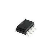
HCPL-J456-500E Avago Technologies US Inc., HCPL-J456-500E Datasheet - Page 14

HCPL-J456-500E
Manufacturer Part Number
HCPL-J456-500E
Description
OPTOCOUPLER 1MBD ALGAAS 8-SMD
Manufacturer
Avago Technologies US Inc.
Datasheet
1.HCPL-4506300.pdf
(21 pages)
Specifications of HCPL-J456-500E
Output Type
Open Collector
Package / Case
8-SMD Gull Wing
Voltage - Isolation
3750Vrms
Number Of Channels
1, Unidirectional
Current - Output / Channel
15mA
Data Rate
1MBd
Propagation Delay High - Low @ If
200ns @ 10mA
Current - Dc Forward (if)
25mA
Input Type
DC
Mounting Type
Surface Mount, Gull Wing
Logic Gate Type
Power Module and Gate Drive Interface Optocouplers
Configuration
1 Channel
Isolation Voltage
3750 Vrms
Current Transfer Ratio
90 %
Maximum Propagation Delay Time
650 ns
Maximum Forward Diode Voltage
1.95 V
Minimum Forward Diode Voltage
1.2 V
Maximum Reverse Diode Voltage
3 V
Maximum Forward Diode Current
20 mA
Maximum Continuous Output Current
15 mA
Maximum Power Dissipation
145 mW
Maximum Operating Temperature
+ 100 C
Minimum Operating Temperature
- 40 C
Number Of Elements
1
Forward Voltage
1.95V
Forward Current
25mA
Output Current
15mA
Package Type
PDIP SMD
Operating Temp Range
-40C to 100C
Power Dissipation
145mW
Propagation Delay Time
650ns
Pin Count
8
Mounting
Surface Mount
Reverse Breakdown Voltage
3V
Operating Temperature Classification
Industrial
Lead Free Status / RoHS Status
Lead free / RoHS Compliant
Lead Free Status / RoHS Status
Lead free / RoHS Compliant, Lead free / RoHS Compliant
Available stocks
Company
Part Number
Manufacturer
Quantity
Price
Company:
Part Number:
HCPL-J456-500E
Manufacturer:
AVAGO
Quantity:
10 000
Part Number:
HCPL-J456-500E
Manufacturer:
AVAGO/安华高
Quantity:
20 000
Notes:
11. Pulse: f = 20 kHz, Duty Cycle = 10%.
12. The internal 20 kΩ resistor can be used by shorting pins 6 and 7 together.
13. Due to tolerance of the internal resistor, and since propagation delay is dependent on the load resistor value, performance can be improved
14. The R
15. See Option 020 data sheet for more information.
16. Use of a 0.1 µF bypass capacitor connected between pins 5 and 8 can improve performance by filtering power supply line noise.
17. The difference between t
18. Common mode transient immunity in a Logic High level is the maximum tolerable dV
19. Common mode transient immunity in a Logic Low level is the maximum tolerable dV
20. Pulse Width Distortion (PWD) is defined as |t
14
Package Characteristics
Over recommended temperature (T
*All typical values at 25°C, V
†The Input-Output Momentary Withstand Voltage is a dielectric voltage rating that should not be interpreted as an input-output continuous
voltage rating. For the continuous voltage rating refer to the IEC/EN/DIN EN 60747-5-2 Insulation Related Characteristics Table (if applicable), your
equipment level safety specification or Avago Application Note 1074 entitled “Optocoupler Input-Output Endurance Voltage, ” publication num-
ber 5963-2203E.
10. This test is performed before the 100% Production test shown in the IEC/EN/DIN EN 60747-5-2 Insulation Related Characteristics Table, if ap-
8. In accordance with UL 1577, each optocoupler is proof tested by applying an insulation test voltage ≥ 4500 V rms for 1 second (leakage
9. In accordance with UL 1577, each optocoupler is proof tested by applying an insulation test voltage ≥ 6000 V rms for 1 second (leakage
1. Derate linearly above 90°C free-air temperature at a rate of 0.8 mA/°C.
2. Derate linearly above 90°C free-air temperature at a rate of 1.6 mA/°C.
3. Derate linearly above 90°C free-air temperature at a rate of 3.0 mW/°C.
4. Derate linearly above 90°C free-air temperature at a rate of 4.2 mW/°C.
5. CURRENT TRANSFER RATIO in percent is defined as the ratio of output collector current (I
6. Device considered a two-terminal device: Pins 1, 2, 3, and 4 shorted together and Pins 5, 6, 7, and 8 shorted together.
7. In accordance with UL 1577, each optocoupler is proof tested by applying an insulation test voltage ≥4500 V rms for 1 second (leakage
Parameter
Input-Output Momentary
Withstand Voltage†
Resistance
(Input-Output)
Capacitance
(Input-Output)
detection current limit, I
detection current limit, I
detection current limit, I
plicable.
by using an external 20 kΩ 1% load resistor. For more information on how propagation delay varies with load resistance, see Figure 8.
Specifications section.)
the output will remain in a Logic High state (i.e., V
the output will remain in a Logic Low state (i.e., V
L
= 20 kΩ, C
L
= 100 pF load represents a typical IPM (Intelligent Power Module) load.
CC
I-O
i-o
I-O
PLH
= 15 V.
≤ 5 µA).
≤5 µA).
≤ 5 µA).
and t
Sym.
V
PHL
C
R
ISO
I-O
I-O
between any two devices under the same test condition. (See IPM Dead Time and Propagation Delay
A
= -40°C to 100°C) unless otherwise specified.
HCNW4506
HCNW4506
HCNW4506
HCPL-4506
HCPL-0466
HCPL-4506
HCPL-4506
HCPL-0466
HCPL-4506
HCPL-0466
HCPL-J456
Option020
HCPL-J456
HCPL-J456
PHL
Device
- t
O
O
< 1.0 V).
PLH
> 3.0 V).
| for any given device.
3750
3750
5000
5000
10
Min.
12
Typ.*
10
10
0.6
0.8
0.5
12
13
Max.
CM
CM
V rms
Units
/dt of the common mode pulse, V
/dt of the common mode pulse, V
pF
O
Ω
) to the forward LED input current (I
Test Conditions
RH < 50%
t = 1 min.
T
V
f = 1 MHz
A
I-O
= 25°C
= 500 Vdc
CM
CM
Fig.
, to assure that
, to assure that
F
) times 100.
6,7,10
6,8,10
6,9,10
Note
6,9,
15
6
6


