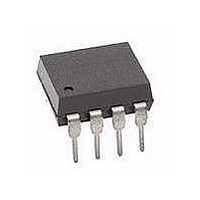
HCNW4503#500 Avago Technologies US Inc., HCNW4503#500 Datasheet

HCNW4503#500
Specifications of HCNW4503#500
Available stocks
Related parts for HCNW4503#500
HCNW4503#500 Summary of contents
Page 1
... Power transistor isolation in motor drives • Line receivers • Feedback element in switched mode power supplies • High speed logic ground isolation – TTL/TTL, TTL/CMOS, TTL/LSTTL • Replaces pulse transformers • Replaces slow phototransistor isolators • Analog signal ground isolation = 1500 V CM for 1 minute (5000 V rms ...
Page 2
The HCPL-4502, HCPL-0452, and HCNW4502 provide the electrical and switching performance of the 6N136, HCPL- 0501, and HCNW136 with increased ESD protection. The HCPL-4503, HCPL-0453, and HCNW4503 are similar to the HCPL-4502, HCPL-0452, and HCNW4502 optocouplers but have increased common ...
Page 3
Ordering Information HCPL-4502 and HCPL-4503, HCPL-0452, HCPL-0453 are UL Recognized with 3750 Vrms for 1 minute per UL1577. HCNW4502 and HCNW4503 are UL Recognized with 5000 Vrms for 1 minute per UL1577. All devices above listed are approved under CSA ...
Page 4
Package Outline Drawings 8-Pin DIP Package (HCPL-4502/3) 9.65 ± 0.25 (0.380 ± 0.010 TYPE NUMBER A XXXXZ YYWW 1.78 (0.070) MAX. 1.19 (0.047) MAX. 3.56 ± 0.13 (0.140 ± 0.005) ...
Page 5
Small Outline SO-8 Package (HCPL-0452/ 5.994 ± 0.203 (0.236 ± 0.008) XXX 3.937 ± 0.127 YWW (0.155 ± 0.005) PIN ONE 0.406 ± 0.076 1.270 (0.016 ± 0.003) (0.050) * 5.080 ± ...
Page 6
Widebody DIP Package with Gull Wing Surface Mount Option 300 (HCNW4502/3) 11.15 ± 0.15 (0.442 ± 0.006 (0.354 ± 0.006 1.55 (0.061) MAX. 1.78 ± 0.15 (0.070 ± 0.006) 2.54 (0.100) ...
Page 7
Recommended Pb-Free IR Profile * 260 +0/-5°C Tp 217°C TL RAMP-UP 3°C/SEC. MAX. 150 - 200°C T smax T smin ts PREHEAT 60 to 180 SEC 25°C to PEAK TIME Regulatory Information The devices contained in this data ...
Page 8
IEC/EN/DIN EN 60747-5-2 Insulation Related Characteristics (OPTION 060 ONLY) Description Installation classification per DIN VDE 0110/1.89, Table 1 for rated mains voltage ≤300 V rms for rated mains voltage ≤450 V rms Climatic Classification Pollution Degree (DIN VDE 0110/1.89) Maximum ...
Page 9
Absolute Maximum Ratings Parameter Storage Temperature Operating Temperature Average Forward Input Current Peak Forward Input Current (50% duty cycle pulse width) (50% duty cycle pulse width) Peak Transient Input Current (≤1 µs pulse width, 300 pps) ...
Page 10
Electrical Specifications (DC) Over recommended temperature (T A Parameter Symbol Device Current CTR HCPL-4502/3 Transfer Ratio HCPL-0452/3 HCNW4502/3 Logic Low V HCPL-4502/3 OL Output Voltage HCPL-0452/3 HCNW4502/3 Logic High I OH Output Current Logic Low I CCL Supply Current Logic ...
Page 11
Switching Specifications (AC) Over recommended temperature (T Parameter Sym. Device Propagation t HCPL-4502/3 PHL Delay Time to HCPL-0452/3 Logic Low at HCNW4502/3 Output Propagation t HCPL-4502/3 PLH Delay Time to HCPL-0452/3 Logic High at HCNW4502/3 Output Common Mode |CM | ...
Page 12
Package Characteristics Over recommended temperature (T Parameter Sym. Device Input-Output V 8-Pin DIP ISO Momentary SO-8 Withstand Widebody Voltage** 8-Pin DIP (Option 020) I 8-Pin DIP I-O Input-Output R 8-Pin DIP I-O Resistance SO-8 Widebody Input-Output C 8-Pin DIP I-O ...
Page 13
PIN DIP, SO 25° 5 OUTPUT VOLTAGE - V O Figure 1. DC and pulsed transfer characteristics. 8 PIN DIP, SO-8 1.5 HCPL-4502/3, HCPL-0452/0453 1.0 ...
Page 14
PIN DIP, SO-8 1.1 1.0 NORMALIZED 25°C A 0.7 HCPL-4502/3, HCPL-0452/0453 0.6 -60 - ...
Page 15
PIN DIP -75 -50 - TEMPERATURE - °C ...
Page 16
1 PHL PLH Figure 10. Switching test circuit 10% 90% 90% 10 ...


