HCPL-T250-300E Avago Technologies US Inc., HCPL-T250-300E Datasheet
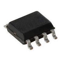
OPTOCOUPLER DRIVER 1.5A 8-SMD GW

HCPL-T250-300E

Manufacturer Part Number
HCPL-T250-300E
Description
OPTOCOUPLER DRIVER 1.5A 8-SMD GW
Manufacturer
Avago Technologies US Inc.
Datasheet

Specifications of HCPL-T250-300E

Voltage - Isolation
3750Vrms
Number Of Channels
1, Unidirectional
Current - Output / Channel
1.5A
Propagation Delay High - Low @ If
270ns @ 7mA ~ 16mA
Current - Dc Forward (if)
25mA
Input Type
DC
Output Type
Push-Pull, Totem-Pole
Mounting Type
Surface Mount, Gull Wing
Package / Case
8-SMD Gull Wing
No. Of Channels
1
Optocoupler Output Type
Gate Drive
Input Current
16mA
Output Voltage
30V
Opto Case Style
SMD
No. Of Pins
8
Peak Reflow Compatible (260 C)
Yes
Isolation Voltage
3.75kV
Number Of Elements
1
Forward Voltage
1.8V
Forward Current
20mA
Package Type
PDIP SMD
Operating Temp Range
-20C to 85C
Power Dissipation
250mW
Propagation Delay Time
500ns
Pin Count
8
Mounting
Surface Mount
Reverse Breakdown Voltage
5V
Operating Temperature Classification
Commercial
Lead Free Status / RoHS Status
Lead free / RoHS Compliant
Lead Free Status / RoHS Status
Lead free / RoHS Compliant, Lead free / RoHS Compliant

Available stocks

Company
Part Number
Manufacturer
Quantity
Price
Part Number:
HCPL-T250-300E
Manufacturer:
AVAGO
Quantity:
45 000
Part Number:
HCPL-T250-300E
Manufacturer:
AVAGO/安华高
Quantity:
20 000
Description
The HCPL‑T250 contains GaAs LED. The LED is optically
coupled to an integrated circuit with a power output stage.
This optocoupler is ideally suited for driving power IGBTs
and MOSFETs used in motor control inverter applications.
The high operating voltage range of the output stage
provides the drive voltages required by gate controlled
devices. The voltage and current supplied by this optocou‑
pler makes it ideally suited for directly driving IGBTs with
ratings up to 1200 V/25 A. For IGBTs with higher ratings,
the HCPL‑T250 can be used to drive a discrete power stage
which drives the IGBT gate.
HCPL-T250
1.5 Amp Output Current IGBT Gate Drive Optocoupler
Data Sheet
Functional Diagram
A 0.1 µF bypass capacitor must be connected between pins 5 and 8.
RoHS 6 fully compliant options available;
-xxxE denotes a lead-free product
CATHODE
ANODE
Lead (Pb) Free
RoHS 6 fully
compliant
N/C
N/C
CAUTION: It is advised that normal static precautions be taken in handling and assembly
of this component to prevent damage and/or degradation which may be induced by ESD.
1
2
3
4
Truth Table
OFF
LED
ON
SHIELD
HIGH
LOW
V
out
Q1
Q2
8
7
6
5
V
V
V
V
CC
O
O
EE
Features
• Input threshold current (I
• Supply current (I
• Supply voltage (V
• Output current (I
• Switching time (t
• Isolation voltage (V
• UL 1577 recognized: File No. E55361
• CSA approved
• IEC/EN/DIN EN 60747‑5‑2 approved with V
• 5 kV/µs Minimum Common Mode Rejection (CMR) at
• Creepage distance: 7.4 mm
Applications
• IGBT/MOSFET gate drive
• AC/brushless DC motor drives
• Industrial inverters
• Switch mode power supplies
V
Vcm = 1500 V
Clearance: 7.1 mm
peak
CC
O
PLH
CC
): ±0.5 A (min.)
): 11 mA (max.)
ISO
): 15‑35 V
/t
PHL
): 3750 Vrms (min.)
): 0.5 µs (max.)
FLH
): 5 mA (max.)
IORM
= 630

Related parts for HCPL-T250-300E

HCPL-T250-300E Summary of contents

Page 1

... The voltage and current supplied by this optocou‑ pler makes it ideally suited for directly driving IGBTs with ratings up to 1200 V/25 A. For IGBTs with higher ratings, the HCPL‑T250 can be used to drive a discrete power stage which drives the IGBT gate. Functional Diagram ...

Page 2

... To order, choose a part number from the part number column and combine with the desired option from the op‑ tion column to form an order entry. Example 1: HCPL‑T250‑560E to order product of 300 mil DIP Gull Wing Surface Mount package in Tape and Reel packaging with IEC/EN/DIN EN 60747‑5‑2 Safety Approval in RoHS compliant. Example 2: HCPL‑ ...

Page 3

Package Outline Drawings Standard DIP Package 9.65 ± 0.25 (0.380 ± 0.010 PIN ONE 1.19 (0.047) MAX. 3.56 ± 0.13 (0.140 ± 0.005) PIN ONE 1.080 ± 0.320 (0.043 ± 0.013) Gull Wing Surface ...

Page 4

Solder Reflow Thermal Profile 300 PREHEATING RATE 3°C + 1°C/–0.5°C/SEC. REFLOW HEATING RATE 2.5°C ± 0.5°C/SEC. 200 160°C 150°C 140°C 3°C + 1°C/–0.5°C 100 PREHEATING TIME 150° SEC. ROOM TEMPERATURE Note: Non-halide flux should ...

Page 5

... Solder Reflow Temperature Profile Notes: 1. Maximum pulse width = 10 µs, maximum duty cycle = 0.2%. See HCPL‑3120 Applications section for additional details on limiting I 2. Derate linearly above 70°C free‑air temperature at a rate of 0.3 mA/°C. 3. Derate lineraly above 70°C free‑air temperature at a rate of 4.8 mW/°C. ...

Page 6

... Recommended Operating Conditions Parameter Symbol Power Supply Voltage V CC Input Current (ON) Input Voltage (OFF Electrical Specifications (Compared with HCPL‑3120) Over recommended operating conditions ( Ground) unless otherwise specified. EE Parameter Symbol Units Input Forward V F Voltage Temperature ∆V /∆T mV/° Coefficient of Forward Voltage ...

Page 7

... CC EE Notes: 4. The difference between t and t between any two HCPL‑3120 parts under the same test condition. PHL PLH 5. Common mode transient immunity in the high state is the maximum tolerable dV output will remain in the high state (i.e Common mode transient immunity in a low state is the maximum tolerable dV put will remain in a low state (i.e., V < ...

Related keywords