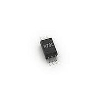
ACPL-W70L-000E Avago Technologies US Inc., ACPL-W70L-000E Datasheet - Page 7

ACPL-W70L-000E
Manufacturer Part Number
ACPL-W70L-000E
Description
OPTOCOUPLER 2CH 15MBD CMOS 6SSOP
Manufacturer
Avago Technologies US Inc.
Datasheet
1.ACPL-W70L-500E.pdf
(14 pages)
Specifications of ACPL-W70L-000E
Input Type
DC
Package / Case
6-SSOP
Voltage - Isolation
5000Vrms
Number Of Channels
1, Unidirectional
Current - Output / Channel
10mA
Data Rate
15MBd
Propagation Delay High - Low @ If
23ns @ 6mA
Current - Dc Forward (if)
10mA
Output Type
Push-Pull, Totem-Pole
Mounting Type
Surface Mount
Isolation Voltage
5000 Vrms
Maximum Continuous Output Current
10 mA
Maximum Fall Time
3.5 ns
Maximum Forward Diode Current
10 mA
Maximum Rise Time
3.5 ns
Minimum Forward Diode Voltage
1.2 V
Output Device
Logic Gate Photo IC
Configuration
1 Channel
Maximum Baud Rate
15 MBps
Maximum Forward Diode Voltage
1.85 V
Maximum Reverse Diode Voltage
5 V (Min)
Maximum Input Diode Current
6 mA
Maximum Power Dissipation
600 mW
Maximum Operating Temperature
+ 105 C
Minimum Operating Temperature
- 40 C
Lead Free Status / RoHS Status
Lead free / RoHS Compliant
Lead Free Status / RoHS Status
Lead free / RoHS Compliant, Lead free / RoHS Compliant
Available stocks
Company
Part Number
Manufacturer
Quantity
Price
Company:
Part Number:
ACPL-W70L-000E
Manufacturer:
Avago Technologies
Quantity:
135
Switching Specifications
Over recommended temperature (T
All typical specifications are at T
Package Characteristics
All Typical at T
Notes:
1. Slew rate of supply voltage ramping is recommended to ensure no glitch more than 1V to appear at the output pin.
2. t
3. PWD is defined as |t
4. t
5. CM
6. CM
7
Parameter
Propagation Delay Time
to Logic Low Output
Propagation Delay Time
to Logic High Output
Pulse Width
Pulse Width Distortion
Propagation Delay Skew
Output Rise Time
(10% – 90%)
Output Fall Time
(90% - 10%)
Common Mode Transient Immunity
at Logic High Output
Common Mode Transient Immunity
at Logic Low Output
Parameter
Input-Output Insulation
Input-Output Momentary
Withstand Voltage
Input-Output Resistance
Input-Output Capacitance
t
recommended operating conditions.
PHL
PLH
PSK
H
L
is equal to the magnitude of the worst case difference in t
propagation delay is measured from the 50% level on the rising edge of the input pulse to the 50% level on the falling edge of the V
propagation delay is measured from the 50% level on the falling edge of the input pulse to the 50% level on the rising edge of the V
is the maximum tolerable rate of fall of the common mode voltage to assure that the output will remain in a low logic state.
is the maximum tolerable rate of rise of the common mode voltage to assure that the output will remain in a high logic state.
A
= 25°C.
PHL
[6]
[2]
[5]
[2]
[3]
- t
[4]
PLH
|.
A
=+25°C, V
A
Symbol
t
t
t
|PWD|
t
t
t
| CM
| CM
Symbol
I
V
R
C
= –40°C to +105°C), 3.0V≤V
I-O
PHL
PLH
PW
PSK
R
F
ISO
I-O
I-O
H
L
|
DD
|
= +3.3V.
Min.
66.7
0
10
10
Min.
5000
PHL
and/or t
Typ.
23
27
4
3.5
3.5
15
15
Typ.
10
0.6
PLH
12
DD
that will be seen between units at any given temperature within the
≤ 3.6V and 4.5 V ≤V
Max.
55
55
25
40
Max.
1.0
Units
ns
ns
ns
ns
ns
ns
ns
kV/μs
kV/μs
Units
μA
V
:
pF
rms
Test Conditions
I
CMOS Signal Levels
I
CMOS Signal Levels
I
CMOS Signal Levels
I
CMOS Signal Levels
I
CMOS Signal Levels
I
CMOS Signal Levels
V
V
Test Conditions
45% RH, t = 5 s
V
T
RH ≤ 50%, t = 1 min.,
T
V
f = 1 MHz, T
DD
F
F
F
F
F
F
A
A
CM
CM
I-O
I-O
= 6 mA, C
= 6 mA, C
= 6 mA, C
= 6 mA, C
= 6 mA, C
= 0 mA, C
= 25°C
= 25°C
≤ 5.5 V.
= 3 kV DC,
= 1000 V, T
= 1000 V, T
= 500 V dc
A
L
L
L
L
L
L
= 15pF
= 15pF
= 15pF
= 15pF
= 15pF
= 15pF
= 25°C
A
A
= 25°C, I
= 25°C, I
F
F
= 6 mA
= 0 mA
O
O
signal.
signal.


