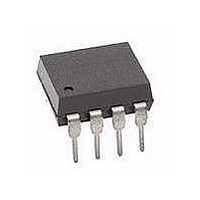
HCNW3120#500 Avago Technologies US Inc., HCNW3120#500 Datasheet - Page 9

HCNW3120#500
Manufacturer Part Number
HCNW3120#500
Description
OPTOCOUPLER 1CH 2.5A 8-SMD
Manufacturer
Avago Technologies US Inc.
Datasheet
1.HCPL-3120-500E.pdf
(24 pages)
Specifications of HCNW3120#500
Output Type
Gate Driver
Package / Case
8-SMD (400 mil) Gull Wing
Voltage - Isolation
5000Vrms
Number Of Channels
1, Unidirectional
Current - Output / Channel
2.5A
Propagation Delay High - Low @ If
300ns @ 7mA ~ 16mA
Current - Dc Forward (if)
25mA
Input Type
DC
Mounting Type
Surface Mount, Gull Wing
Configuration
1 Channel
Isolation Voltage
5000 Vrms
Maximum Propagation Delay Time
500 ns
Maximum Forward Diode Voltage
1.95 V
Minimum Forward Diode Voltage
1.2 V
Maximum Reverse Diode Voltage
3 V
Maximum Forward Diode Current
16 mA
Maximum Power Dissipation
295 mW
Maximum Operating Temperature
+ 100 C
Minimum Operating Temperature
- 40 C
Number Of Elements
1
Forward Voltage
1.95V
Forward Current
25mA
Package Type
PDIP W SMD
Operating Temp Range
-40C to 100C
Power Dissipation
295mW
Propagation Delay Time
500ns
Pin Count
8
Mounting
Surface Mount
Reverse Breakdown Voltage
5V
Operating Temperature Classification
Industrial
Lead Free Status / RoHS Status
Contains lead / RoHS non-compliant
Lead Free Status / RoHS Status
Lead free / RoHS Compliant, Contains lead / RoHS non-compliant
Available stocks
Company
Part Number
Manufacturer
Quantity
Price
Absolute Maximum Ratings
Parameter
Storage Temperature
Operating Temperature
Average Input Current
Peak Transient Input Current
(<1 µs pulse width, 300 pps)
Reverse Input Voltage
“High” Peak Output Current
“Low” Peak Output Current
Supply Voltage
Input Current (Rise/Fall Time)
Output Voltage
Output Power Dissipation
Total Power Dissipation
Lead Solder Temperature
Solder Reflow Temperature Profile
Recommended Operating Conditions
Parameter
Power Supply Voltage
Input Current (ON)
Input Voltage (OFF)
Operating Temperature
9
HCPL-3120
HCPL-J312
HCNW3120
HCPL-3120
HCPL-J312
HCNW3120
HCPL-3120
HCPL-J312
HCNW3120
(V
I
V
T
F(ON)
Symbol
A
F(OFF)
CC
- V
EE
)
T
T
I
I
V
I
I
(V
t
V
P
P
260°C for 10 sec., 1.6 mm below seating plane
260°C for 10 sec., up to seating plane
See Package Outline Drawings section
F(AVG)
F(TRAN)
OH(PEAK)
OL(PEAK)
Symbol
r(IN)
A
S
R
O(PEAK)
O
T
CC
Min.
15
7
10
-3.6
-40
- V
/t
f(IN)
EE
)
Max.
30
16
0.8
100
Min.
-55
-40
0
0
Units
Volts
mA
V
°C
Max.
125
100
25
1.0
5
5
2.5
2.5
35
500
V
250
295
CC
Units
°C
°C
mA
A
Volts
A
A
Volts
ns
Volts
mW
mW
Note
1
2
2
3
4


