4N33M Fairchild Optoelectronics Group, 4N33M Datasheet - Page 4
4N33M
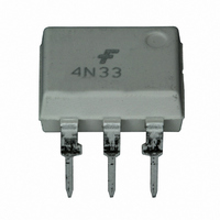
Manufacturer Part Number
4N33M
Description
OPTOCOUPLER PHOTODARLINGTON 6DIP
Manufacturer
Fairchild Optoelectronics Group
Datasheet
1.H11B1SR2M.pdf
(10 pages)
Specifications of 4N33M
Number Of Channels
1
Input Type
DC
Voltage - Isolation
1500Vrms
Current Transfer Ratio (min)
500% @ 10mA
Voltage - Output
30V
Current - Output / Channel
150mA
Current - Dc Forward (if)
80mA
Vce Saturation (max)
1V
Output Type
Darlington with Base
Mounting Type
Through Hole
Package / Case
6-DIP
Lead Free Status / RoHS Status
Lead free / RoHS Compliant
Current Transfer Ratio (max)
-
Available stocks
Company
Part Number
Manufacturer
Quantity
Price

Part Number:
4N33M
Manufacturer:
FAIRCHILD/仙童
Quantity:
20 000


©2007 Fairchild Semiconductor Corporation
4NXXM, H11B1M, TIL113M Rev. 1.0.3
Electrical Characteristics
Isolation Characteristics
* Indicates JEDEC registered data.
Notes:
1. The current transfer ratio(I
2. Pulse test: pulse width = 300µs, duty cycle
3. I
4. The frequency at which I
5. For this test, LED pins 1 and 2 are common, and phototransistor pins 4, 5 and 6 are common.
Safety and Insulation Ratings
As per IEC 60747-5-2, this optocoupler is suitable for “safe electrical insulation” only within the safety limit data.
Compliance with the safety ratings shall be ensured by means of protective circuits.
Symbol
Symbol
F
V
R
C
V
V
adjusted to I
V
RIO
CTI
ISO
IORM
ISO
ISO
IOTM
PR
Input-Output Isolation Voltage
Isolation Resistance
Isolation Capacitance
Installation Classifications per DIN VDE 0110/1.89
Table 1
For Rated Main Voltage < 150Vrms
For Rated Main voltage < 300Vrms
Climatic Classification
Pollution Degree (DIN VDE 0110/1.89)
Comparative Tracking Index
Input to Output Test Voltage, Method b,
V
with tm = 1 sec, Partial Discharge < 5pC
Input to Output Test Voltage, Method a,
V
with tm = 60 sec, Partial Discharge < 5pC
Max. Working Insulation Voltage
Highest Allowable Over Voltage
External Creepage
External Clearance
Insulation Thickness
Insulation Resistance at Ts, V
IORM
IORM
C
= 2.0mA and I
Characteristic
x 1.875 = V
x 1.5 = V
C
C
is 3dB down from the 1kHz value.
/I
PR
F
(5)
) is the ratio of the detector collector current to the LED input current.
PR
, Type and Sample Test
C
(5)
Parameter
= 0.7mA rms.
, 100% Production Test
(T
A
= 25°C Unless otherwise specified.) (Continued)
(5)
IO
f = 60Hz, t = 1 sec.
VDC
VDC
V
V
I-O
I-O
= 500V
2.0% .
Test Conditions
= 500VDC
= Ø, f = 1MHz
4
Min.
1594
1275
6000
175
850
10
0.5
4N32M*
4N33M*
Device
7
7
9
All
All
All
55/100/21
Min.
7500
2500
1500
Typ.
10
I-IV
I-IV
2
11
Typ.
0.8
Max.
Max.
www.fairchildsemi.com
V
AC
Units
V
V
V
V
Unit
mm
mm
mm
pF
PEAK
peak
peak
peak
peak
V
Related parts for 4N33M
Image
Part Number
Description
Manufacturer
Datasheet
Request
R

Part Number:
Description:
OPTOCOUPLER DARL-OUT 6-DIP
Manufacturer:
Fairchild Optoelectronics Group
Datasheet:

Part Number:
Description:
LED 7-SEG SGL CC RED RHDP .3"
Manufacturer:
Fairchild Optoelectronics Group
Datasheet:

Part Number:
Description:
LED IR EMITTING 940NM SIDELOOKER
Manufacturer:
Fairchild Optoelectronics Group
Datasheet:
Part Number:
Description:
LED IR EMITTING GAAS 940NM 3MM
Manufacturer:
Fairchild Optoelectronics Group
Datasheet:
Part Number:
Description:
LED IR EMITTING ALGAAS 880NM 3MM
Manufacturer:
Fairchild Optoelectronics Group
Datasheet:
Part Number:
Description:
LED IR EMITTING 940NM SMD 2MM
Manufacturer:
Fairchild Optoelectronics Group
Datasheet:
Part Number:
Description:
IC PHOTOTRANS IR 940NM BLK 1.9MM
Manufacturer:
Fairchild Optoelectronics Group
Datasheet:
Part Number:
Description:
LED IR GAAS SIDELOOK 940NM
Manufacturer:
Fairchild Optoelectronics Group
Datasheet:
Part Number:
Description:
LED IR EMITTING 940NM 2MM SMD
Manufacturer:
Fairchild Optoelectronics Group
Datasheet:
Part Number:
Description:
IC PHOTOTRANS IR 940NM 1.9MM GW
Manufacturer:
Fairchild Optoelectronics Group
Datasheet:
Part Number:
Description:
LED 7-SEG SGL CC RED RHDP .3"
Manufacturer:
Fairchild Optoelectronics Group
Datasheet:

Part Number:
Description:
DIODE EMITTING GAAS IRED TO-46
Manufacturer:
Fairchild Optoelectronics Group
Datasheet:
Part Number:
Description:
DIODE EMITTING GAAS IRED TO-46
Manufacturer:
Fairchild Optoelectronics Group
Datasheet:

Part Number:
Description:
LED SS BIPO RED/GRN DIFF PCB 5MM
Manufacturer:
Fairchild Optoelectronics Group
Datasheet:

Part Number:
Description:
LED SS HI EFF GREEN DIFF 3MM
Manufacturer:
Fairchild Optoelectronics Group
Datasheet: