6N138 Fairchild Optoelectronics Group, 6N138 Datasheet
6N138
Specifications of 6N138
Available stocks


Related parts for 6N138


6N138 Summary of contents
Page 1
... GND 4 5 N/C 6N138 / 6N139 ©2005 Fairchild Semiconductor Corporation 6N138, 5N139, NCPL2730, HCPL2731 Rev. 1.0.5 Description The 6N138/9 and HCPL2730/HCPL2731 optocouplers consist of an AlGaAs LED optically coupled to a high gain split darlington photodetector. The split darlington configuration separating the input photodiode and the fi ...
Page 2
... Emitter-Base Reverse Voltage Supply Voltage, Output Voltage Output Power Dissipation O ©2005 Fairchild Semiconductor Corporation 6N138, 5N139, NCPL2730, HCPL2731 Rev. 1.0 25°C unless otherwise specified) A Parameter Each Channel Each Channel Each Channel Each Channel Each Channel 6N138 and 6N139 6N138, HCPL2730 ...
Page 3
... Transfer Characteristics Symbol Parameter COUPLED CTR Current Transfer (1)(2) Ratio V Logic LOW Output OL (2) Voltage *All Typicals 25°C A ©2005 Fairchild Semiconductor Corporation 6N138, 5N139, NCPL2730, HCPL2731 Rev. 1.0 70°C unless otherwise specified) A Test Conditions T = 25°C A Each channel (I = 1.6mA 25° 10µ ...
Page 4
... Transient R Immunity at Logic (3) HIGH (Fig. 25) |CM | Common Mode (I L Transient T Immunity at Logic (3) LOW (Fig. 25) ** All Typicals 25°C A ©2005 Fairchild Semiconductor Corporation 6N138, 5N139, NCPL2730, HCPL2731 Rev. 1.0.5 (Continued 70°C unless otherwise specified 5V) CC Test Conditions = 4 0.5mA 25° 4 0.5mA 25° 270 , I ...
Page 5
... Current Transfer Ratio is defined as a ratio of output collector current times 100 Pin 7 open. (6N138 and 6N139 only) 3. Common mode transient immunity in logic HIGH level is the maximum tolerable (positive) dV leading edge of the common mode pulse signal V (i.e., V > 2.0V). Common mode transient immunity in logic LOW level is the maximum tolerable (negative) ...
Page 6
... Load Current Through L Resistor Input Current of Output Gate 2 V DD1 Fig. 2 Non-Inverting Logic Interface ©2005 Fairchild Semiconductor Corporation 6N138, 5N139, NCPL2730, HCPL2731 Rev. 1.0.5 (Continued 25°C unless otherwise specified) A OL1 CMOS INPUT R1 ( (V) CMOS NON-INV. 2000 1000 @ 5V INV. 510 CMOS NON-INV ...
Page 7
... A 0.1 0. 25˚ 0˚C A 0.001 1.0 1.1 1.2 1.3 FORWARD VOLTAGE - V Fig. 6 Non-saturated Rise and Fall Times vs. Load Resistance (6N138 / 6N139 Only) 100 T = 25˚ ADJUSTED FOR 0 LOAD RESISTANCE ( Fig. 8 Propagation Delay To Logic Low vs. Base-Emitter Resistance (HCPL2730 / HCPL2731 Only) ...
Page 8
... T = 85˚ 70˚ 25˚ 0˚ -40˚ 0.01 0 INPUT DIODE FORWARD CURRENT -mA ©2005 Fairchild Semiconductor Corporation 6N138, 5N139, NCPL2730, HCPL2731 Rev. 1.0.5 (Continued) Fig. 11 Current Transfer Ratio vs. Forward Current 5000 4000 3000 2000 1000 I = 1.6mA 0 100 1000 0.1 Fig. 13 Output Current vs Output Voltage 120 4 ...
Page 9
... Fig. 20 Propagation Delay to Logic Low vs. Pulse Period (6N138 / 6N139 Only) 100 6N139 I = 0.5mA 4.7k L 6N138 I = 1.6mA 2.2k L 0.1 0.01 0 INPUT PULSE PERIOD - ms ©2005 Fairchild Semiconductor Corporation 6N138, 5N139, NCPL2730, HCPL2731 Rev. 1.0.5 (Continued) 100 18V Fig. 19 Propagation Delay vs. Input Diode Forward Current 4 ...
Page 10
... HCPL2730 : I = 1 HCPL2731 : I = 0 (HCPL2731) PLH (HCPL2731) PHL 10 t (HCPL2730) PHL TEMPERATURE (˚C) A ©2005 Fairchild Semiconductor Corporation 6N138, 5N139, NCPL2730, HCPL2731 Rev. 1.0.5 (Continued) 50 HCPL2730 : I HCPL2731 : (HCPL2730) PLH Fig. 23 Propagation Delay vs. Temperature (HCPL2730 / HCPL2731 Only) = 1.6mA 2. 0.5mA 4. (HCPL2731) PLH t ...
Page 11
... I/ < 100ns 3 I Monitor Test Circuit for 6N138, 6N139 I F Noise Shield Pulse Gen Test Circuit for 6N138 and 6N139 ©2005 Fairchild Semiconductor Corporation 6N138, 5N139, NCPL2730, HCPL2731 Rev. 1.0.5 Pulse Generator 5ns Z = 50V 10% DUTY CYCLE I/f < 100 µ 0.1 µF MONITOR Rm ...
Page 12
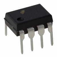
... TYP Lead Coplanarity : 0.004 (0.10) MAX Note: All dimensions are in inches (millimeters) ©2005 Fairchild Semiconductor Corporation 6N138, 5N139, NCPL2730, HCPL2731 Rev. 1.0.5 0.4" Lead Spacing 0.200 (5.08) 0.140 (3.55) 15 MAX 0.300 (7.62) TYP 0.022 (0.56) 0.016 (0.41) 8-Pin DIP – ...
Page 13
... SDV Marking Information Definitions ©2005 Fairchild Semiconductor Corporation 6N138, 5N139, NCPL2730, HCPL2731 Rev. 1.0.5 Example Part Number 6N138 Standard Through Hole Device, 50 pcs per tube 6N138S Surface Mount Lead Bend 6N138SD Surface Mount; Tape and reel 6N138W 0.4" Lead Spacing 6N138V ...
Page 14
... MAX User Direction of Feed Reflow Profile 300 250 200 150 100 ©2005 Fairchild Semiconductor Corporation 6N138, 5N139, NCPL2730, HCPL2731 Rev. 1.0.5 12.0 0.1 4.0 0.1 4.0 0.1 0.05 10.30 0.20 225C peak Time above 183C, 60–150 sec ...
Page 15
... Product Status Advance Information Formative / In Design Preliminary First Production No Identification Needed Full Production Obsolete Not In Production ©2005 Fairchild Semiconductor Corporation 6N138, 5N139, NCPL2730, HCPL2731 Rev. 1.0.5 PDP SPM™ FPS™ F-PFS™ Power-SPM™ ® FRFET PowerTrench SM Programmable Active Droop™ ...