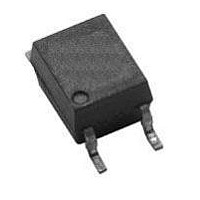
HCPL-M453-500E Avago Technologies US Inc., HCPL-M453-500E Datasheet - Page 6

HCPL-M453-500E
Manufacturer Part Number
HCPL-M453-500E
Description
OPTOCOUPLER 1CH 1MBS SO-5
Manufacturer
Avago Technologies US Inc.
Datasheet
1.HCPL-M452500.pdf
(9 pages)
Specifications of HCPL-M453-500E
Number Of Channels
1
Input Type
DC
Voltage - Isolation
3750Vrms
Current Transfer Ratio (min)
20% @ 16mA
Current Transfer Ratio (max)
50% @ 16mA
Voltage - Output
20V
Current - Output / Channel
8mA
Current - Dc Forward (if)
25mA
Output Type
Transistor with Vcc
Mounting Type
Surface Mount
Package / Case
5-SOP
No. Of Channels
1
Optocoupler Output Type
Phototransistor
Input Current
16mA
Output Voltage
20V
Opto Case Style
SOIC
No. Of Pins
5
Ctr Max
50%
Isolation Voltage
3.75kV
Lead Free Status / RoHS Status
Lead free / RoHS Compliant
Vce Saturation (max)
-
Lead Free Status / Rohs Status
Compliant
Available stocks
Company
Part Number
Manufacturer
Quantity
Price
Company:
Part Number:
HCPL-M453-500E
Manufacturer:
AVAGO
Quantity:
26 000
Part Number:
HCPL-M453-500E
Manufacturer:
AVAGO/安华高
Quantity:
20 000
Part Number:
HCPL-M453-500E/HCPLM453-500E
Manufacturer:
AVAGO/安华高
Quantity:
20 000
Switching Specifications
Over recommended temperature (T
All typicals at T
Notes:
1. Derate linearly above 85°C free-air temperature at a rate of 0.5 mA/°C.
2. Derate linearly above 85°C free-air temperature at a rate of 1.0 mA/°C.
3. Derate linearly above 85°C free-air temperature at a rate of 1.1 mW/°C.
4. Derate linearly above 85°C free-air temperature at a rate of 2.3 mW/°C.
5. CURRENT TRANSFER RATIO in percent is defined as the ratio of output collector current, I
6. Device considered a two terminal device: pins 1 and 3 shorted together, and pins 4, 5 and 6 shorted together.
7. In accordance with UL 1577, each optocoupler is proof tested by applying an insulation test voltage ≥ 4500 V
8. Common transient immunity in a Logic High level is the maximum tolerable (positive) dV
9. The 1.9 k: load represents 1 TTL unit load of 1.6 mA and the 5.6 k: pull-up resistor.
10. The frequency at which the ac output voltage is 3 dB below its mid-frequency value.
11. Use of a 0.1 PF bypass capacitor con nected between pins 4 and 6 is recommended.
6
Parameter
Propagation Delay
Time to Logic Low
at Output
Propagation Delay
Time to Logic High
at Output
Common Mode
Transient Immunity
at Logic High Level
Output
Common Mode
Transient Immunity
at Logic Low Level
Output
Bandwidth
current limit, I
to assure that the output will remain in a Logic High state (i.e., V
tolerable (negative) dV
(i.e., V
O
< 0.8 V).
A
= 25°C.
I-O
≤ 5 PA).
Symbol
t
t
|CM
|CM
BW
CM
PHL
PLH
/dt on the falling edge of the common mode pulse signal, V
H
L
|
|
Device
HCPL-
M452
HCPL-
M453
HCPL-
M452
HCPL-
M453
A
= 0°C to 70°C) V
Min.
15
15
Typ.*
0.2
0.6
1
30
1
30
3
CC
O
> 2.0 V). Common mode transient immunity in a Logic Low level is the maximum
= 5 V, I
Max.
0.8
1.0
0.8
1.0
F
= 16 mA unless otherwise specified.
Units
Ps
kV/Ps
MHz
CM
CM
O
to assure that the output will remain in a Logic Low state
, to the forward LED input current, I
Test Conditions
T
T
V
V
V
V
V
V
R
/dt on the rising edge of the common mode pulse, V
A
A
CM
CM
p-p
CM
CM
p-p
L
= 25°C
= 25°C
= 100 :, See Test Circuit
= 10 V
= 1500
= 10 V
= 1500
p-p
p-p
R
R
I
T
R
I
T
R
F
F
A
A
L
L
L
L
RMS
= 0 mA
= 16 mA
= 1.9 k:
= 1.9 k:
= 25°C
= 1.9 k:
= 25°C
= 1.9 k:
for 1 second (leakage detection
Fig.
5, 6, 10
5, 6, 10
11
11
8, 9
F
, times 100.
9
9
10
Note
8, 9
8, 9
CM
,


