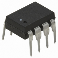
HCPL-4562 Avago Technologies US Inc., HCPL-4562 Datasheet - Page 10

HCPL-4562
Manufacturer Part Number
HCPL-4562
Description
OPTOCOUPLER HI BAND 17MHZ 8DIP
Manufacturer
Avago Technologies US Inc.
Datasheet
1.HCPL-4562-000E.pdf
(17 pages)
Specifications of HCPL-4562
Input Type
DC
Package / Case
8-DIP (0.300", 7.62mm)
Number Of Channels
1
Voltage - Isolation
3750Vrms
Voltage - Output
20V
Current - Output / Channel
8mA
Current - Dc Forward (if)
12mA
Output Type
Transistor with Vcc
Mounting Type
Through Hole
Isolation Voltage
3750 Vrms
Minimum Forward Diode Voltage
1.1 V
Output Device
Phototransistor
Configuration
1 Channel
Current Transfer Ratio
45 %
Maximum Forward Diode Voltage
1.6 V
Maximum Reverse Diode Voltage
1.8 V
Maximum Input Diode Current
12 mA
Maximum Power Dissipation
100 mW
Maximum Operating Temperature
+ 85 C
Minimum Operating Temperature
- 40 C
Lead Free Status / RoHS Status
Contains lead / RoHS non-compliant
Vce Saturation (max)
-
Current Transfer Ratio (max)
-
Current Transfer Ratio (min)
-
Lead Free Status / RoHS Status
Lead free / RoHS Compliant, Contains lead / RoHS non-compliant
Other names
516-1052-5
Available stocks
Company
Part Number
Manufacturer
Quantity
Price
Company:
Part Number:
HCPL-4562
Manufacturer:
AGILENT
Quantity:
500
Company:
Part Number:
HCPL-4562#500
Manufacturer:
AGILENT
Quantity:
500
Company:
Part Number:
HCPL-4562-000E
Manufacturer:
AVAGO
Quantity:
10 000
Company:
Part Number:
HCPL-4562-020E
Manufacturer:
TI
Quantity:
1 200
Company:
Part Number:
HCPL-4562-020E
Manufacturer:
AVAGO
Quantity:
10 000
Package Characteristics
All Typicals at T
*The Input-Output Momentary Withstand Voltage is a dielectric voltage rating that should not be interpreted as an input-output continuous voltage
rating. For the continuous voltage rating refer to the VDE 0884 Insulation Related Characteristics Table (if applicable), your equipment level safety
specification or Avago Application Note 1074 entitled “Optocoupler Input-Output Endurance Voltage, ” publication number 5963-2203E.
Notes:
10. TOTAL HARMONIC DISTORTION (THD) is defined as the square root of the sum of the square of each harmonic distortion component. The THD
11. ISOLATION MODE REJECTION RATIO (IMRR), a measure of the optocoupler’s ability to reject signals or noise that may exist between input and
12. In accordance with UL 1577, each optocoupler is proof tested by applying an insulation test voltage ≥4500 V rms for 1 second (leakage detec-
13. In accordance with UL 1577, each optocoupler is proof tested by applying an insulation test voltage ≥6000 V rms for 1 second (leakage detec-
10
1. When used in the circuit of Figure 1 or Figure 4; G
2. Derate linearly above 70°C free-air temperature at a rate of 2.0 mW/°C (HCPL-4562).
3. Maximum variation from the best fit line of I
4. CURRENT TRANSFER RATIO (CTR) is defined as the ratio of output collector current, I
5. Device considered a two-terminal device: Pins 1, 2, 3, and 4 shorted together and Pins 5, 6, 7, and 8 shorted together.
6. Flat-band, small-signal voltage gain.
7. The frequency at which the gain is 3 dB below the flat-band gain.
8. Differential gain is the change in the small-signal gain of the optocoupler at 3.58 MHz as the bias level is varied over a given range.
9. Differential phase is the change in the small-signal phase response of the optocoupler at 3.58 MHz as the bias level is varied over a given
Parameter
Input-Output
Momentary
Withstand
Voltage*
Input-Output
Resistance
Input-Output
Capacitance
range.
of the isolated video circuit is measured using a 2.6 kΩ load in series with the 50 Ω input impedance of the spectrum analyzer.
output terminals, is defined by 20 log
tion current limit, I
Characteristics Table, if applicable.
tion current limit, I
Characteristics Table, if applicable.
A
= 25°C
I-O
I-O
≤5 µA). This test is performed before the 100% Production test shown in the IEC/EN/DIN EN 60747-5-2 Insulation Related
≤5 µA). This test is performed before the 100% Production test shown in the IEC/EN/DIN EN 60747-5-2 Insulation Related
Sym.
V
R
C
ISO
I-O
I-O
(Option 020)
HCNW4562
HCNW4562
HCNW4562
HCPL-4562
HCPL-4562
HCPL-4562
HCPL-4562
Device
10
[(V
OUT
PB
/V
vs. I
IN
)/(V
V
F
= V
expressed as a percentage of the peak-to-peak full scale output.
OUT
3750
5000
5000
Min.
10
10
OUT
/V
12
11
/V
IM
)], where V
IN
; I
FQ
= 6 mA (HCPL-4562), I
10
10
Typ.
0.6
0.5
12
13
IM
is the isolation mode voltage signal.
Max.
0.6
O
, to the forward LED input current, I
FQ
V rms
Units
= 10 mA (HCNW4562).
pF
Ω
Test Conditions
RH ≤50%,
t = 1 min.,
T
V
T
T
f = 1 MHz
A
A
A
I-O
= 25°C
= 25°C
= 100°C
= 500 Vdc
F
, times 100%.
Fig.
5, 12
5, 13
5, 13
Note
5
5


