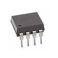
HCNW4562#500 Avago Technologies US Inc., HCNW4562#500 Datasheet

HCNW4562#500
Specifications of HCNW4562#500
Available stocks
Related parts for HCNW4562#500
HCNW4562#500 Summary of contents
Page 1
HCPL-4562, HCNW4562 High Bandwidth, Analog/Video Optocouplers Data Sheet Description The HCPL-4562 and HCNW4562 optocouplers provide wide bandwidth isolation for analog signals. They are ideal for video isolation when combined with their application circuit (Figure 4). High linearity and low phase ...
Page 2
Selection Guide Single Channel Packages 8-Pin DIP (300 Mil) HCPL-4562 Ordering Information HCPL-4562 is UL Recognized with 3750 Vrms for 1 minute per UL1577 unless otherwise specified. HCNW4562 is UL Recognized with 5000 Vrms for 1 minute per UL1577. Option ...
Page 3
Package Outline Drawings 8-Pin DIP Package (HCPL-4562) 9.65 ± 0.25 (0.380 ± 0.010 TYPE NUMBER A XXXXZ R YYWW 1.19 (0.047) MAX. 3.56 ± 0.13 (0.140 ± 0.005) 1.080 ± 0.320 (0.043 ± 0.013) ...
Page 4
Widebody DIP Package (HCNW4562) 11.15 ± 0.15 (0.442 ± 0.006 HCNWXXXX YYWW 2.54 (0.100) TYP. 1.78 ± 0.15 (0.070 ± 0.006) 8-Pin Widebody DIP Package with Gull Wing Surface Mount Option 300 ...
Page 5
Solder Reflow Temperature Profile 300 PREHEATING RATE 3°C + 1°C/–0.5°C/SEC. REFLOW HEATING RATE 2.5°C ± 0.5°C/SEC. 200 160°C 150°C 140°C 3°C + 1°C/–0.5°C 100 PREHEATING TIME 150° SEC. ROOM TEMPERATURE Note: Non-halide flux should ...
Page 6
Insulation and Safety Related Specifications Parameter Symbol Minimum External L(101) Air Gap (External Clearance) Minimum External L(102) Tracking (External Creepage) Minimum Internal Plastic Gap (Internal Clearance) Minimum Internal Tracking (Internal Creepage) Tracking Resistance CTI (Comparative Tracking Index) Isolation Group Option ...
Page 7
Absolute Maximum Ratings Parameter Storage Temperature Operating Temperature Average Forward Input Current Peak Forward Input Current Effective Input Current Reverse LED Input Voltage (Pin 3-2) Input Power Dissipation Average Output Current (Pin 6) Peak Output Current (Pin 6) Emitter-Base Reverse ...
Page 8
Electrical Specifications (DC 25° for HCPL-4562 and Parameter Symbol Device Base Photo I PB Current HCPL-4562 I ∆ Temperature ∆T Coefficient I HCPL-4562 PB Nonlinearity HCNW4562 Input Forward ...
Page 9
Small Signal Characteristics (AC 25° for HCPL-4562 and Parameter Symbol Voltage Gain G HCPL-4562 V (0.1 MHz) HCNW4562 G Temperature ∆G /∆ Coefficient Base Photo ∆i HCPL-4562 PB Current ...
Page 10
Package Characteristics All Typicals 25°C A Parameter Sym. Device Input-Output V HCPL-4562 ISO Momentary HCNW4562 Withstand HCPL-4562 Voltage* (Option 020) Input-Output R HCPL-4562 I-O Resistance HCNW4562 Input-Output C HCPL-4562 I-O Capacitance HCNW4562 *The Input-Output Momentary Withstand Voltage ...
Page 11
Figure 1. Gain and bandwidth test circuit Figure 2. Base photo current test circuit Figure 4. Recommended isolated video interface circuit 11 162 Ω (HCPL-4562) 90.9 Ω (HCNW4562) Figure 3. Base photo current frequency ...
Page 12
HCPL-4562 100 – ° ° -10 °C A 0.1 0.01 1.0 1.1 1.2 1.3 1.4 V – FORWARD VOLTAGE – Figure ...
Page 13
HCPL-4562 1.04 1.02 1.00 0.98 NORMALIZED 0. ° 0.92 V > 0.90 0.88 0.86 - ...
Page 14
HCPL-4562 -10 ° ° ° NORMALIZED - ° 0.1 MHz -6 -7 0.01 0.1 1.0 ...
Page 15
HCPL-4562 150 °C A 120 -20 dB/DECADE SLOPE IMRR = 20 LOG OUT IM 0 0.01 0.1 1.0 10 100 1000 10,000 f – FREQUENCY – KHz Figure ...
Page 16
Conversion from HCPL-4562 to HCNW4562 In order to obtain similar circuit performance when converting from the HCPL-4562 to the HCNW4562 recommended to increase the Quiescent Input Current from mA. If the application ...
Page 17
For product information and a complete list of distributors, please go to our website: Avago, Avago Technologies, and the A logo are trademarks of Avago Technologies Limited in the United States and other countries. Data subject to change. Copyright © ...


