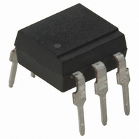
4N46-060E Avago Technologies US Inc., 4N46-060E Datasheet

4N46-060E
Specifications of 4N46-060E
Available stocks
Related parts for 4N46-060E
4N46-060E Summary of contents
Page 1
... The 4N46 has a 350% minimum CTR at an input current of only 0.5 mA making it ideal for use in low input current applications such as MOS, CMOS and low power logic interfacing. Compatibility with high ...
Page 2
... Ordering Information 4N45/4N46 are UL Recognized with 3750 Vrms for 1 minute per UL1577 and is approved under CSA Component Acceptance Notice #5, File CA 88324. Option Part RoHS non RoHS Number Compliant Compliant Package -000E no option 300 mil DIP-6 -300E -300 300 mil DIP-6 4N45 ...
Page 3
Outline Drawing 9.40 (0.370) 9.90 (0.390 XXXX YYWW RU PIN 1 2 ONE DOT 1.78 (0.070) MAX. 2.16 (0.085) 2.54 (0.100) DIMENSIONS IN MILLIMETERS AND (INCHES). Outline Drawing – Option 300 9.65 ± 0.25 (0.380 ± 0.010) ...
Page 4
Solder Reflow Thermal Profile 300 PREHEATING RATE 3°C + 1°C/–0.5°C/SEC. REFLOW HEATING RATE 2.5°C ± 0.5°C/SEC. 200 160°C 150°C 140°C 3°C + 1°C/–0.5°C 100 PREHEATING TIME 150° SEC. ROOM TEMPERATURE Note: Non-halide flux should ...
Page 5
... Regulatory Information The 4N45 and 4N46 have been approved by the following regulatory organizations: UL Recognized under UL 1577, Component Recognition Program, File E55361. Insulation and Safety Related Specifications Parameter Min. External Air Gap (External Clearance) Min. External Tracking Path (External Creepage) Min. Internal Plastic Gap ...
Page 6
... Peak Transient Input Current Reverse Input Voltage, V ...................................................................... Input Power Dissipation, P ........................................................ Output Current, I (Pin 5) ........................................................... Emitter-Base Reverse Voltage (Pins 4-6) .......................................... 0.5 V Output Voltage, V (Pin 5-4) O 4N45 ........................................................................................... -0 4N46 .........................................................................................-0 Output Power Dissipation ......................................................... 100 mW Infrared and Vapor Phase Reflow Temperature (Option #300) .............................................. see Fig. 1, Thermal Profile 6 Symbol V IORM IOTM T S ...
Page 7
... Recommended Operating Conditions Parameter Symbol Output Voltage (4N46) Output Voltage (4N45) Input Current (High) I Input Voltage (Low) V Operating Temperature DC Electrical Specifications Over recommended temperature (T A Parameter Device Symbol Current Transfer 4N46 Ratio 4N45 Logic Low 4N46 Output Voltage 4N45 Logic High ...
Page 8
Package Characteristics For unless otherwise specified. All typicals Parameter Symbol Input-Output Momentary V Withstand Voltage* Resistance, Input-Output R Capacitance, Input-Output C *The Input-Output Momentary Withstand Voltage is a dielectric voltage rating that ...
Page 9
Figure 8. Propagation delay vs. load resistor. Figure 10. Test circuit for transient immunity and typical waveforms. Figure 11. External base resistor Figure 9. Switching test circuit. Figure 12. Effect of ...
Page 10
Applications TTL Interface Line Voltage Monitor Analog Signal Isolation 10 Telephone Ring Detector CMOS Interface ...
Page 11
For product information and a complete list of distributors, please go to our website: Avago, Avago Technologies, and the A logo are trademarks of Avago Technologies Limited in the United States and other countries. Data subject to change. Copyright © ...


