TLP181(GB,F,T) Toshiba, TLP181(GB,F,T) Datasheet - Page 35
TLP181(GB,F,T)
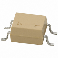
Manufacturer Part Number
TLP181(GB,F,T)
Description
PHOTOCOUPLER TRANS-OUT 4-SMD
Manufacturer
Toshiba
Specifications of TLP181(GB,F,T)
Number Of Channels
1
Input Type
DC
Voltage - Isolation
3750Vrms
Current Transfer Ratio (min)
100% @ 5mA
Current Transfer Ratio (max)
600% @ 5mA
Voltage - Output
80V
Current - Output / Channel
50mA
Current - Dc Forward (if)
50mA
Vce Saturation (max)
400mV
Output Type
Transistor
Mounting Type
Surface Mount
Package / Case
4-SMD
Configuration
1 Channel
Maximum Collector Emitter Voltage
80 V
Maximum Collector Emitter Saturation Voltage
0.4 V
Isolation Voltage
3750 Vrms
Current Transfer Ratio
100 % to 600 %
Maximum Forward Diode Voltage
1.3 V
Minimum Forward Diode Voltage
1 V
Maximum Power Dissipation
200 mW
Maximum Operating Temperature
+ 100 C
Minimum Operating Temperature
- 55 C
Forward Current
10 mA
Maximum Input Diode Current
10 mA
Output Device
Phototransistor
Number Of Elements
1
Reverse Breakdown Voltage
5V
Forward Voltage
1.3V
Collector-emitter Voltage
80V
Package Type
MFSOP
Collector Current (dc) (max)
50mA
Power Dissipation
200mW
Collector-emitter Saturation Voltage
0.4V
Pin Count
4
Mounting
Surface Mount
Operating Temp Range
-25C to 85C
Operating Temperature Classification
Commercial
Lead Free Status / RoHS Status
Lead free / RoHS Compliant
Other names
TLP181GBF


Triac-Output Photocouplers for Solid State Relays ( SSRs ) (Continued)
Triac-Output Photocouplers for Office Equipment
Triac-Output Photocouplers for AC 100 to 120 V Lines
Note 2: BSI and IEC: : Approved (supplementary or basic insulation)
TLP260J
TLP261J
TLP360J
TLP360JF
TLP361J
TLP361JF
TLP363J
TLP363JF
TLP525G
TLP525G-2
TLP525G-4
TLP560G
Part Number
Part Number
Part Number
TÜV and VDE: : Approved
For the latest information, please contact your nearest Toshiba sales representative.
EN 60065- and IEC 60065-approved, EN 60950- and IEC 60950-approved
EN 60747-5-2-approved with option V4 or D4
16
1
Pin Configuration
Pin Configuration
Pin Configuration
8
1
15
2
6
1
14
3
6
1
6
1
4
1
4
1
4
1
4
1
7
2
13
4
2
12
5
ZC
ZC
ZC
6
3
4
3
4
3
3
2
3
2
3
2
3
2
11
6
: Design which meets safety standard/approval pending as of January 2011
4
3
10
7
5
4
9
8
DIP4
DIP6
General-purpose
Non-zero cross
DIP8
Dual-channel version
of the TLP525G
DIP16
4-channel version
of the TLP525G
Mini-flat
MFSOP6
Non-zero cross
Mini-flat
MFSOP6
Zero cross
DIP4
Non-zero cross
DIP4
Zero cross
DIP4
Zero cross
High impulse noise
immunity
V
N
= 2000 V (typ.)
Features
Features
Features
: Approved (reinforced insulation)
Rank
Rank
Rank
IFT7
IFT7
IFT7
IFT5
−
−
−
−
−
−
−
−
−
I
I
I
FT
FT
FT
(Max)
(Max)
(Max)
10 mA
10 mA
10 mA
10 mA
10 mA
10 mA
10 mA
10 mA
10 mA
7 mA
7 mA
7 mA
5 mA
35
2.8 V
2.8 V
2.8 V
2.8 V
2.8 V
3 V
3 V
3 V
3 V
V
V
V
TM
TM
TM
(Max)
(Max)
(Max)
100 mA 400 V
100 mA 400 V
100 mA 400 V
100 mA 400 V
70 mA
70 mA
70 mA
: Design which meets safety standard/approval pending as of January 2011
70 mA
70 mA
@I
@I
@I
TM
TM
TM
600 V
600 V
600 V
600 V
600 V
V
V
V
DRM
DRM
DRM
Vrms
Vrms
Vrms
Vrms
Vrms
5000
5000
5000
2500
Vrms
2500
Vrms
2500
Vrms
2500
Vrms
3000
3000
BVs
BVs
BVs
UL/c-UL
UL/c-UL
UL/c-UL
/
/
/
/ –
/ –
/
/
/
/ –
TÜV
TÜV
TÜV
Safety Standards
Safety Standards
Safety Standards
VDE
VDE
VDE
(1)
(1)
BSI
BSI
BSI
(2)
(2)
(2)
IEC
IEC
IEC
Related parts for TLP181(GB,F,T)
Image
Part Number
Description
Manufacturer
Datasheet
Request
R

Part Number:
Description:
PHOTOCOUPLER TRANS OUT 4-SMD
Manufacturer:
Toshiba
Datasheet:

Part Number:
Description:
PHOTOCOUPLER TRANS OUT 6MFSOP-4
Manufacturer:
Toshiba
Datasheet:
Part Number:
Description:
PHOTOCOUPLER TRANS-OUT 4-SMD
Manufacturer:
Toshiba
Datasheet:
Part Number:
Description:
Transistor Output Optocouplers 80Vceo 3750Vrms High CTR
Manufacturer:
Toshiba
Part Number:
Description:
IC OPTOCOUPL AC/DC-IN 1-CH TRANS DC-OUT 4MFSOP
Manufacturer:
Toshiba
Datasheet:
Part Number:
Description:
GaAs IRED & PHOTO-TRANSISTOR
Manufacturer:
Toshiba
Datasheet:
Part Number:
Description:
PHOTOCOUPLER TRANS-OUT 4-SMD
Manufacturer:
Toshiba
Datasheet:
Part Number:
Description:
PHOTOCOUPLER TRANS-OUT 4-SMD
Manufacturer:
Toshiba
Datasheet:
Part Number:
Description:
PHOTOCOUPLER TRANS OUT 4-SMD
Manufacturer:
Toshiba
Datasheet:
Part Number:
Description:
PHOTOCOUPLER TRANS OUT 4-SMD
Manufacturer:
Toshiba
Datasheet:
Part Number:
Description:
PHOTOCOUPLER TRANS OUT 4-SMD
Manufacturer:
Toshiba
Datasheet:
Part Number:
Description:
PHOTOCOUPLER TRANS OUT 4-SMD
Manufacturer:
Toshiba
Datasheet:
Part Number:
Description:
PHOTOCOUPLER TRANS OUT 4-SMD
Manufacturer:
Toshiba
Datasheet:
Part Number:
Description:
PHOTOCOUPLER TRANS OUT 4-SMD
Manufacturer:
Toshiba
Datasheet: