HCMS-2914 Avago Technologies US Inc., HCMS-2914 Datasheet - Page 9
HCMS-2914
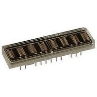
Manufacturer Part Number
HCMS-2914
Description
LED DISPLAY 5X7 8CHAR 3.8MM ORN
Manufacturer
Avago Technologies US Inc.
Series
HCMS-29xxr
Datasheet
1.HCMS-2903.pdf
(16 pages)
Specifications of HCMS-2914
Millicandela Rating
*
Size / Dimension
1.40" L x 0.40" W x 0.20" H (35.6mm x 10.2mm x 5.1mm)
Color
Orange
Configuration
5 x 7
Voltage - Forward (vf) Typ
*
Package / Case
26-DIP
Display Type
Alphanumeric
Number Of Digits/alpha
8
Digit/alpha Size
0.15" (3.8mm)
Character Format
Dot Matrix
Character Size
3.81mm
Led Color
Orange
Luminous Intensity
64µcd
No. Of Digits / Alpha
8
Display Area Width
35.56mm
Display Area Height
10.16mm
Number Of Digits
8
Illumination Color
Orange
Wavelength
600 nm
Operating Voltage
- 0.3 V to 5.5 V
Maximum Operating Temperature
+ 85 C
Minimum Operating Temperature
- 40 C
Lead Free Status / RoHS Status
Lead free / RoHS Compliant
Common Pin
-
Lead Free Status / Rohs Status
Details


HCMS-29xx Write Cycle Diagram
Control Register
The Control Register allows software modification of the
IC’s operation and consists of two independent 7-bit
control words. Bit D
the two 7-bit control words. Control Word 0 performs
pulse width modulation brightness control, peak pixel
current brightness control, and sleep mode. Control Word
1 sets serial/simultaneous data out mode, and external
oscillator prescaler. Each function is independent of
the others.
Control Register Data Loading
Data is loaded into the Control Register, MSB first, ac-
cording to the procedure shown in Table 1 and the
Write Cycle Timing Diagram. First, RS is brought to logic
high and then CE is brought to logic low. Next, each
successive rising CLK edge will shift in the data on the
D
line is brought to logic high. When CLK goes to logic
low, new data is copied into the selected control word.
Loading data into the Control Register takes place while
the previous control word configures the display.
9
(SIMULTANEOUS)
IN
LED OUTPUTS,
D
pin. Finally, when 8 bits have been loaded, the CE
OUT
REGISTERS
CONTROL
(SERIAL)
D
CLK
OUT
D
CE
RS
IN
NOTE:
1. DATA IS COPIED TO THE CONTROL REGISTER OR THE DOT LATCH AND LED OUTPUTS WHEN CE IS HIGH AND CLK IS LOW.
T
CLKCE
T
3
RSS
1
7
in the shift register selects one of
T
T
CEDO
RSH
10
2
T
CES
4
T
DOUTP
9
T
DS
6
T
T
DOUT
DH
7
8
T
CLKH
11
PREVIOUS DATA
T
CLKL
12
Control Word 0
Loading the Control Register with D
lects Control Word 0 (see Table 2). Bits D
display brightness by pulse width modulating the LED
on-time, while Bits D
by changing the peak pixel current. Bit D
operation or sleep mode.
Sleep mode (Control Word 0, bit D
Internal Display Oscillator and the LED pixel drivers. This
mode is used when the IC needs to be powered up, but
does not need to be active. Current draw in sleep mode
is nearly zero. Data in the Dot Register and Control Words
are retained during sleep mode.
4
-D
5
adjust the display brightness
T
CEH
5
NEW DATA LATCHED HERE
6
= Low) turns off the
7
= Logic low se-
6
0
selects normal
-D
3
adjust the
NEW DATA
[1]
Related parts for HCMS-2914
Image
Part Number
Description
Manufacturer
Datasheet
Request
R

Part Number:
Description:
LED DISPLAY 5X7 4CHAR 5MM GREEN
Manufacturer:
Avago Technologies US Inc.
Datasheet:

Part Number:
Description:
LED DISPLAY 5X7 8CHAR 3.8MM YLW
Manufacturer:
Avago Technologies US Inc.
Datasheet:

Part Number:
Description:
LED DISPLAY 5X7 4CHAR 3.8MM YLW
Manufacturer:
Avago Technologies US Inc.
Datasheet:

Part Number:
Description:
LED DISPLAY 5X7 4CHAR 3.8MM ORN
Manufacturer:
Avago Technologies US Inc.
Datasheet:

Part Number:
Description:
LED DISPL 5X7 4CHAR 3.8MM ALGAAS
Manufacturer:
Avago Technologies US Inc.
Datasheet:
Part Number:
Description:
LED DISPLAY 5X7 4CHAR 3.8MM RED
Manufacturer:
Avago Technologies US Inc.
Datasheet:
Part Number:
Description:
LED DISPLAY 5X7 4CHAR 3.8MM ORN
Manufacturer:
Avago Technologies US Inc.
Datasheet:
Part Number:
Description:
LED DISPLAY 5X7 4CHAR 3.8MM YLW
Manufacturer:
Avago Technologies US Inc.
Datasheet:
Part Number:
Description:
LED DISPLAY 5X7 4CHAR 5MM YLW
Manufacturer:
Avago Technologies US Inc.
Datasheet:
Part Number:
Description:
LED DISPLAY 5X7 4CHAR 5MM ORN
Manufacturer:
Avago Technologies US Inc.
Datasheet:
Part Number:
Description:
LED DISPLAY 5X7 4CHAR 5MM GRN
Manufacturer:
Avago Technologies US Inc.
Datasheet:
Part Number:
Description:
LED DISPLAY 5X7 4CHAR 5MM RED
Manufacturer:
Avago Technologies US Inc.
Datasheet:
Part Number:
Description:
LED DISPLAY 5X7 4CHAR 3.8MM RED
Manufacturer:
Avago Technologies US Inc.
Datasheet:
Part Number:
Description:
LED DISPLAY 5X7 4CHAR 3.8MM GRN
Manufacturer:
Avago Technologies US Inc.
Datasheet:
Part Number:
Description:
LED DISPLAY 5X7 4CHAR 5MM GRN
Manufacturer:
Avago Technologies US Inc.
Datasheet: