HDSP2115S OSRAM Opto Semiconductors Inc, HDSP2115S Datasheet - Page 11
HDSP2115S
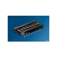
Manufacturer Part Number
HDSP2115S
Description
DISPLAY 8CHAR .200" ORANGE
Manufacturer
OSRAM Opto Semiconductors Inc
Series
Intelligent Display®r
Datasheet
1.HDSP2110S.pdf
(16 pages)
Specifications of HDSP2115S
Millicandela Rating
150µcd
Size / Dimension
1.70" L x 0.77" W x 0.21" H (42.67mm x 19.58mm x 5.31mm)
Color
Orange
Configuration
5 x 7
Number Of Digits
8
Character Size
0.2 in
Illumination Color
Soft Orange
Wavelength
610 nm
Maximum Operating Temperature
+ 85 C
Minimum Operating Temperature
- 40 C
Luminous Intensity
270 ucd
Viewing Area (w X H)
2.85 mm x 4.81 mm
Display Type
5 x 7 Dot Matrix
Lead Free Status / RoHS Status
Lead free / RoHS Compliant
Voltage - Forward (vf) Typ
-
Internal Connection
-
Lead Free Status / Rohs Status
Details
Other names
Q68000A8907


UDC Address Register
The UDC Address Register is selected by setting FL=1, A4=0,
A3=0. It is a 4 bit register and uses data bits, D3–D0 to store the
4 bit address code (D7–D4 are ignored). The address code selects
one of 16 UDC RAM locations for custom character generation.
UDC RAM
The UDC RAM is selected by setting FL=1, A4=0, A3=1. The RAM
is comprised of a 7 x 5 bit RAM. As shown in Table „Flash RAM
Access Logic“ (page 12), address lines, A2–A0 select one of the
7 rows of the custom character. Data bits, D4–D0 determine the
5 bits of column data in each row. Each data bit corresponds to a
LED. If the data bit is high, then the LED is on. If the data bit is low,
the LED is off. To create a character, each of the 7 rows of column
data need to be defined. See Tables „UDCAddress Register and
UDC Character RAM“ (page 11) and „UDC Character Map“
(page 12) for logic.
Flash RAM
The Flash RAM allows the display to flash one or more of the char-
acters being displayed. The Flash Ram is accessed by setting FL
low. A4 and A3 are ignored. The Flash RAM is a 8 x 1 bit RAM with
each bit corresponding to a digit address. Digit 0 is on the left side
of the display and digit 7 is on the right side of the display. Address
lines, A2–A0 select the digit address with A2 being the most signif-
icant digit and A0 being the least significant digit. Data bit, D0, sets
and resets the flash bit for each digit. When D0 is high, the flash bit
is set and when D0 is low, It is reset. See Table „Flash RAM
Access Logic“ (page 12).
Character RAM Access Logic
RST
1
1
1
1
UDC Address Register and UDC Character RAM
RST
1
1
1
1
2006-01-23
HSDP2110S, HSDP2111S, HSDP2112S, HSDP2113S, HSDP2114S, HSDP2115S
CE
0
0
0
0
CE
0
0
0
0
WR
0
1
0
1
WR
0
1
0
1
RD
1
0
1
0
RD
1
0
1
0
FL
1
1
1
1
FL
1
1
1
1
A4
1
1
0
0
A4
0
0
0
0
A3
1
1
0
0
A3
0
0
1
1
A2
Character Address for Digits 0–7
Character Address for Digits 0–7
Character Address for Digits 0–7
Character Address for Digits 0–7
A2
Not used for UDC
Address Register
Not used for UDC
Address Register
A2–A0=Character
Row Address
A2–A0=Character
Row Address
A1
A1
A0
A0
11
Control Word
The Control Word is used to set up the attributes required by the
user. It is addressed by setting FL=1, A4=1, A3=0. The Control
Word is an 8 bit register and is accessed using data bits, D7–D0.
See Table „Control Word Access Logic“ (page 12) and Figure
„Control Word Data Definition“ (page 13) for the logic and attrib-
uted control. The Control Word has 5 functions. They are bright-
ness control, flashing character enable, blinking character enable,
self test, and clear (Flash and Character RAMS only).
Brightness Control
Control Word bits, D2–D0, control the brightness of the display
with a binary code of 000 being 100% brightness and 111 being
display blank. See Figure „Control Word Data Definition“ (page 13)
for brightness level versus binary code. The average I
calculated by multiplying the 100% brightness level I
the display’s brightness level. For example, a display set to 80%
brightness with a 100% average I
average I
Flash Function
Control Word bit, D3, enables or disables the Flash Function.
When D3 is 1, the Flash Function is enabled and any digit with its
corresponding bit set in the Flash RAM will flash at approximately
2.0 Hz. When using an external clock, the flash rate can be deter-
mined by dividing the clock rate by 28,672. When D3 is 0, the
Flash Function is disabled and the contents of the Flash RAM is
ignored. For synchronized flashing on multiple displays, see the
Reset Section (page 12)..
D7 D6 D5 D4 D3 D2 D1 D0
D3–D0=UDC RAM Address Code for Write
Cycle
D3–D0=UDC RAM Address Code for Read
Cycle
D4–D0=Character Column Data for
Write Cycle
D4–D0=Character Column Data read
during a Read Cycle
CC
value of 200 mA x 80%=160 mA.
D7 D6 D5 D4 D3 D2 D1 D0
0 7 bit ASCII code for a Write Cycle
0 7 bit ASCII code read during a Read Cycle
1
1 D3–D0=UDC address for Read Data
D3–D0=UDC address for a Write Cycle
CC
value of 200 mA will have an
CC
CC
value by
UDC
Address
Register
UDC
RAM
can be
Related parts for HDSP2115S
Image
Part Number
Description
Manufacturer
Datasheet
Request
R

Part Number:
Description:
INTELLIGENT DISP 4CHAR 5X7 HERED
Manufacturer:
OSRAM Opto Semiconductors Inc
Datasheet:

Part Number:
Description:
DISPLAY 8DIGIT CERAMIC GREEN
Manufacturer:
OSRAM Opto Semiconductors Inc
Datasheet:

Part Number:
Description:
EMITTER IR 950NM 5MM SMD RADIAL
Manufacturer:
OSRAM Opto Semiconductors Inc
Datasheet:

Part Number:
Description:
LED TOPLED GREEN 570NM 2-PLCC
Manufacturer:
OSRAM Opto Semiconductors Inc
Datasheet:

Part Number:
Description:
INTERRUPTER RELFECT W/FILTR SMD
Manufacturer:
OSRAM Opto Semiconductors Inc
Datasheet:

Part Number:
Description:
LED Displays 5x7 Green 0.145 , 4-CHARACTER
Manufacturer:
OSRAM Opto Semiconductors Inc
Datasheet:

Part Number:
Description:
Q65110A4321_SIDELED PURE GREEN EOL150407
Manufacturer:
OSRAM Opto Semiconductors Inc
Datasheet:
Part Number:
Description:
Q65110A1202_RO DETECTOR 3/5MM_TR_RO
Manufacturer:
OSRAM Opto Semiconductors Inc
Datasheet:

Part Number:
Description:
PHOTODIODE 900NM 3MM W/FILTER
Manufacturer:
OSRAM Opto Semiconductors Inc
Datasheet:
Part Number:
Description:
INTELLIGENT DISP 4CHAR 5X7 HERED
Manufacturer:
OSRAM Opto Semiconductors Inc
Datasheet:
Part Number:
Description:
LED TOPLED GREEN 570NM 2-PLCC
Manufacturer:
OSRAM Opto Semiconductors Inc
Datasheet:
Part Number:
Description:
PHOTODIODE 900NM 3MM W/FILTER
Manufacturer:
OSRAM Opto Semiconductors Inc
Datasheet:

Part Number:
Description:
PHOTODIODE 850NM THRU-HOLE
Manufacturer:
OSRAM Opto Semiconductors Inc
Datasheet:

Part Number:
Description:
PHOTODIODE 880NM W/FILTER SMD
Manufacturer:
OSRAM Opto Semiconductors Inc
Datasheet: