IPD2548A OSRAM Opto Semiconductors Inc, IPD2548A Datasheet - Page 9
IPD2548A
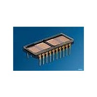
Manufacturer Part Number
IPD2548A
Description
DISPLAY 4CHAR .250" YELLOW
Manufacturer
OSRAM Opto Semiconductors Inc
Series
Alphanumeric Programmable Display™r
Datasheet
1.IPD2545A.pdf
(12 pages)
Specifications of IPD2548A
Millicandela Rating
150µcd
Size / Dimension
1.20" L x 0.49" W x 0.17" H (30.48mm x 12.45mm x 4.32mm)
Color
Yellow
Configuration
5 x 7
Number Of Digits
4
Character Size
0.252 in
Illumination Color
Yellow
Wavelength
585 nm
Maximum Operating Temperature
+ 100 C
Minimum Operating Temperature
- 55 C
Luminous Intensity
150 ucd
Viewing Area (w X H)
4.32 mm x 6.4 mm
Display Type
5 x 7 Dot Matrix
Lead Free Status / RoHS Status
Lead free / RoHS Compliant
Voltage - Forward (vf) Typ
-
Internal Connection
-
Lead Free Status / Rohs Status
Details
Other names
Q68000A9885
Available stocks
Company
Part Number
Manufacturer
Quantity
Price


*“Cursor”= all dots in a single character space lit to half brightness
X = don't care
B = depends on the selected brightness
Attributes are non-destructive. If a character with bit D7 set is
replaced by a cursor (Control Word bit D4 is set, and D3=D2=0)
the character will remain in memory and can be revealed again by
clearing D4 in the Control Word.
Blink (D5): The entire display can be caused to blink at a rate of
approximately 2.0 Hz by setting bit D5 in the Control Word. This blink-
ing is independent of the state of D7 in all character locations.
To synchronize the blink rate in a bank of these devices, it is nec-
essary to tie all devices' clocks and resets together as described in
a later section of this data sheet.
Lamp Test (D6): When the Lamp Test bit is set, all dots in the
entire display are lit at half brightness. When this bit is cleared, the
display returns to the characters that were showing before the
lamp test.
Cascading the Display
2006-03-03
D7 D6 D5 D4 D3 D2 D1 D0 Operation
0
0
0
0
0
D7 D6 D5 D4 D3 D2 D1 D0 Operation
0
0
0
0
0
0
0
RESET
D0-D7
A0-A2
WR
RD
10 µF
0
0
0
0
0
1
A3
A4
A5
0.01 µF
0
1
1
1
1
X
V
X
0
0
1
1
X
CC
1
2
3
6
74LS138
4
X
0
1
0
1
X
8
16
5
12
13
14
15
V
CC
B
B
B
B
B
B
B
B
B
B
B
B
Disable highlight
attribute
Display cursor*
instead of character
Blink single character
Display blinking cur-
sor* instead of char-
acter
Alternate character
with cursor*
Blinking display
0.01 µF
9
Clear Data (D7): When D7 (D7=1) is set in the Control Word, all
display memory bits are reset to zero. A second Control Word must
be written into the chip with D7 (D7=0) reset to set up attributes and
brightness levels.
Cascading
Cascading the display (Figure below) is a simple operation. The
requirements for cascading are:
1) decoding the correct address to determine the chip select for
each additional device,
2) assuring that all devices are reset simultaneously, and
3) selecting one display as the clock source and setting all others
to accept clock input (the reason for cascading the clock is to syn-
chronize the flashing of multiple displays). One display as a source
is capable of driving six other displays. If more displays are
required, a buffer will be necessary. The source display must have
pin 3 tied high to output clock signals. All other displays must have
pin 3 tied low.
Voltage Transients
It has become common practice to provide 0.01 µF bypass capaci-
tors liberally in digital systems. Like other CMOS circuitry, the Intel-
ligent Display controller chip has very low power consumption and
the usual 0.01 µF would be adequate were it not for the LEDs. To
prevent power supply transients, capacitors with low inductance
and high capacitance at high frequencies are required. This sug-
gests a solid tantalum or ceramic disc for high frequency bypass.
For larger displays, distribute the bypass capacitors evenly, keep-
ing capacitors as close to the power pins as possible. We recom-
mend a 10 µF and 0.01 µF for every Intelligent Display to decouple
the displays themselves, at the display.
10 µF
D7 D6 D5 D4 D3 D2 D1 D0 Operation
0
D7 D6 D5 D4 D3 D2 D1 D0 Operation
1
1
0
0.01 µF
IPD2545A, IPD2547A, IPD2548A
0
X
0
X
X
X
X
X
X
X
0.01 µF
X
X
Lamp test
Clear
IDCD5039
Related parts for IPD2548A
Image
Part Number
Description
Manufacturer
Datasheet
Request
R

Part Number:
Description:
INTELLIGENT DISP 4CHAR 5X7 HERED
Manufacturer:
OSRAM Opto Semiconductors Inc
Datasheet:

Part Number:
Description:
DISPLAY 8DIGIT CERAMIC GREEN
Manufacturer:
OSRAM Opto Semiconductors Inc
Datasheet:

Part Number:
Description:
EMITTER IR 950NM 5MM SMD RADIAL
Manufacturer:
OSRAM Opto Semiconductors Inc
Datasheet:

Part Number:
Description:
LED TOPLED GREEN 570NM 2-PLCC
Manufacturer:
OSRAM Opto Semiconductors Inc
Datasheet:

Part Number:
Description:
INTERRUPTER RELFECT W/FILTR SMD
Manufacturer:
OSRAM Opto Semiconductors Inc
Datasheet:

Part Number:
Description:
LED Displays 5x7 Green 0.145 , 4-CHARACTER
Manufacturer:
OSRAM Opto Semiconductors Inc
Datasheet:

Part Number:
Description:
Q65110A4321_SIDELED PURE GREEN EOL150407
Manufacturer:
OSRAM Opto Semiconductors Inc
Datasheet:
Part Number:
Description:
Q65110A1202_RO DETECTOR 3/5MM_TR_RO
Manufacturer:
OSRAM Opto Semiconductors Inc
Datasheet:

Part Number:
Description:
PHOTODIODE 900NM 3MM W/FILTER
Manufacturer:
OSRAM Opto Semiconductors Inc
Datasheet:
Part Number:
Description:
INTELLIGENT DISP 4CHAR 5X7 HERED
Manufacturer:
OSRAM Opto Semiconductors Inc
Datasheet:
Part Number:
Description:
LED TOPLED GREEN 570NM 2-PLCC
Manufacturer:
OSRAM Opto Semiconductors Inc
Datasheet:
Part Number:
Description:
PHOTODIODE 900NM 3MM W/FILTER
Manufacturer:
OSRAM Opto Semiconductors Inc
Datasheet:

Part Number:
Description:
PHOTODIODE 850NM THRU-HOLE
Manufacturer:
OSRAM Opto Semiconductors Inc
Datasheet:

Part Number:
Description:
PHOTODIODE 880NM W/FILTER SMD
Manufacturer:
OSRAM Opto Semiconductors Inc
Datasheet: