CU40025-UW6J Noritake Company Inc, CU40025-UW6J Datasheet
CU40025-UW6J
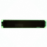
Specifications of CU40025-UW6J
Available stocks


Related parts for CU40025-UW6J


CU40025-UW6J Summary of contents
Page 1
... VACUUM FLUORESCENT DISPLAY SPECIFICATION MODEL: CU40025-UW6J REVISION: F-1 SPECIFICATION NO. : DS-1381-0000- Mar., 27, 2007 (00R PUBLISHED BY This specification is subject to change without prior notice. This product complies with RoHS Directive 2002/95/EC RoHS 2002/95/EC MODULE : May, 7, 2007 (00) : Jun., 23, 2008 (01) : Jul. 17, 2009 (02) : Aug. 21, 2009 (03) NORITAKE ITRON CORP ...
Page 2
... SS V 0.7V IH2 IL2 4.75 5. Symbol Min. "H" -0 "L" V – OL "H" -0 "L" V – – CC1 I – CC2 – 1 CU40025-UW6J Max. Unit − 5 − Max. Unit – – 0.8 – – 0. Typ. Max. Unit – I – 0.6 I – – ...
Page 3
... Shock (Non operation lines x 40 chars dot with underline : 138.8 x 11.5mm ( 2 0.38 x 0.5mm ( 0.48 x 0.7mm ( 350 cd/m (100fL) Min. : Green (Blue-green) : -40 to +85 degree : -50 to +85 degree : (Non condensation) 1.0 mm (Total Amplitude) 30 min. (Duration each direction 2 : 539 m/S , 10mS 2 CU40025-UW6J ...
Page 4
... S/C R CU40025-UW6J Time Description Clears all display 100 µs and Sets DD RAM 0 1 MAX. address 0 in the address counter. Sets DD RAM address 0 in the address counter. Also returns the 1 * 666 ns display being shifted to the original position. DD RAM contents remain unchanged. Sets the cursor ...
Page 5
... Don’t care. CODE 1 ACG ADD ACC Data writing Data reading 8-bits 4-bits Busy Not busy 4 CU40025-UW6J Time Description Sets the CG RAM 666 ns address. Sets the DD RAM 666 ns address. Reads busy flag 666 ns (BF) and address counter. Writes data into ...
Page 6
... S=0 and I/D=1, the cursor would shift one character to the right after a CPU writes to DD RAM. However if S=1 and I/D=1, the display would shift one character to the left and the cursor would maintain its position on the panel I/D 5 CU40025-UW6J 1 01H * 02H to 03H *: Don’t care S 04H to 07H ...
Page 7
... S Shift both cursor and display. S Shift cursor only S/C R CU40025-UW6J After reading DD RAM data The cursor moves one character to the left. The cursor moves one character to the right. The cursor moves one character to the left. The cursor moves one character to the right. B ...
Page 8
... Screen brightness is as follows; BR1 BR0 BR1 BR0 Brightness 100 % ( Default ) CU40025-UW6J Display shift No shift No shift Shift one character to the left Shift one character to the right * 20H to 3FH *: Don’t care 00H to 03H *: Don’t care ...
Page 9
... Once the “Set DD RAM Address” instruction has been executed, the contents of the address counter will be automatically modified after each access of DD RAM, as selected by the “7.4 Entry Mode Set” instruction. Valid DD RAM Address Ranges Number of Characters 1st line 2nd line ACG ADD ADR 40 00H to 27H 40 40H to 67H 8 CU40025-UW6J 40H to 7FH ...
Page 10
... In “Busy Flag Check” immediately after executing “Write Data” instruction, a valid address counter value can be ready as soon as BF goes low. The BF bit shows the status of the busy flag busy ready for next instruction, command receivable. DB4 DB3 DB2 DB1 DB4 DB3 DB2 DB1 ACC 9 CU40025-UW6J 00H to FFH DB0 DB0 ...
Page 11
... Character code DB5 DB4 DB3 DB2 DB1 DB0 DB7 DB6 DB5 DB4 DB3 DB2 DB1 DB0 00H (08H 01H (09H REMARKS; " ": Don't care Dot assignment "0": Turned off "1": Turned on Dot 36 is for underline. 10 CU40025-UW6J CG RAM data (character pattern ...
Page 12
... If 4-bit interface is used, the 8-bit instruction are written nibble by nibble: the high-order nibble being written first, followed by low-order nibble not necessary to check the busy flag between writing separate nibbles of individual instructions. See “ 7.7.1 Function Set Command “ for more information. ), the busy flag (BF) is “1”. 100 µs 11 CU40025-UW6J ...
Page 13
... Write> STB SCK Synchronous bits <Data Read> STB SCK Synchronous bits Start Byte 0 Data Write Instruction Register R Start Byte 1µ R CU40025-UW6J 1 Data Read Data Register Instruction / Data IR6 IR5 IR4 IR3 IR2 Read Data IR1 IR0 ...
Page 14
... The following figure shows the location of each jumper. Location The following table shows the function and JP4, JP2, JP9. CU40025-UW6J is no reset inputs and M68 CPU bus parallel interface at default setting. Reset input signal is active when it is low. Table and JP4 setting ...
Page 15
... Character Font Note: Font number 00-07Hex (08-0FHex) is User Definable Character Fonts. 14 CU40025-UW6J ...
Page 16
... D0∼D7 10.2. CPU bus read timing (Parallel interface i80 type) RS Min 5 nS /RD D0∼D7 Min 250 nS Min 150 nS Min 60 nS Min 5 nS Min 0 nS Valid Min 333 nS Min 130 nS Min 190 nS Max 160 nS Min 5 nS Valid 15 CU40025-UW6J Min 0 nS Min 0 nS ...
Page 17
... CPU bus read timing (Parallel interface M68 type) RS Min R/W D0∼D7 Min 20 nS Min 500 nS Min 230 nS Min 80 nS Valid Min 500 nS Min 230 nS Max 160 nS Valid 16 CU40025-UW6J Min 10 nS Min 230 nS Min 10 nS Min 10 nS Min 230 nS Min 5 nS ...
Page 18
... Min. 100ns Min. 200ns 1 SCK 0 Min. 100ns 10.6 Read timing (Serial interface) 1 STB 0 Min. 200ns 1 SCK 0 Max. 150ns 1 SI/SO 0 Min. 500ns Min. 200ns Min. 100ns Min. 500ns Min. 200ns 17 CU40025-UW6J Min. Min. 500ns 500ns Min. Min. 500ns 500ns Max. 30ns Input ...
Page 19
... Data input Input/Output Data input Input/Output Data input Input/Output Data input Input/Output Data input Input/Output Data input Input/Output Data input Input/Output Data input Input/Output Function Direction Power supply Input Data input/output Input/Output Ground Input Strobe Input Display clock Input Non connection - 18 CU40025-UW6J - ...
Page 20
... CU40025-UW6J ...
Page 21
... If necessary , please ask for assistance from our sales consultant. ・This product is not designed for military, aerospace, medical or other life-critical applications. If you choose to use this product for these applications, please ask us for prior consultation or we cannot take responsibility for problems that may occur. 20 CU40025-UW6J ...