HFBR-2505CZ Avago Technologies US Inc., HFBR-2505CZ Datasheet - Page 6
HFBR-2505CZ
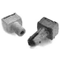
Manufacturer Part Number
HFBR-2505CZ
Description
RCVR FIBER OPTIC INTERBUS-S
Manufacturer
Avago Technologies US Inc.
Datasheet
1.HFBR-2505AZ.pdf
(11 pages)
Specifications of HFBR-2505CZ
Data Rate
2MBd
Voltage - Supply
4.75 V ~ 5.25 V
Current - Supply
6.2mA
Applications
General Purpose
Data Rate Max
0.01Gbps
Data Transmission Distance
400m
Wavelength Typ
650nm
Peak Reflow Compatible (260 C)
Yes
Leaded Process Compatible
Yes
Connector Type
SMA, INTERBUS-S
Lead Free Status / RoHS Status
Lead free / RoHS Compliant
Power - Minimum Receivable
-
Lead Free Status / RoHS Status
Lead free / RoHS Compliant, Lead free / RoHS Compliant


HFBR-25x5AZ/BZ Receivers
The HFBR-25x5AZ/BZ receiver consists of a silicon PIN
photodiode and digitizing IC to produce a logic compat-
ible output. The IC includes a unique circuit to correct
the pulse width distortion of the first bit after a long idle
period. This enables operation from DC to 10 MBd with
low PWD for arbitrary data patterns. The receiver output is
a “push–pull” stage compatible with TTL and CMOS logic.
The receiver housing is a dark grey, conductive plastic.
The HFBR-2505AZ is compatible with SMA connectors,
while the HFBR-2515BZ mates with ST
Absolute Maximum Ratings
Electrical/Optical Characteristics
-0°C to +70°C, 4.75 V < V
Parameter
Peak Input Power Level
Logic HIGH
Peak Input Power Level
Logic LOW
Supply Current
High Level Output
Voltage
Low Level Output Voltage
Output Rise Time
Output Fall Time
Notes:
1. Typical data are at 25˚C, V
2. 1.6 mm below seating plane.
3. In recommended receiver circuit, with an optical signal from the recommended transmitter circuit.
4. Pins 1 and 4 are electrically connected to the conductive housing and are also used for mounting and retaining purposes. It is required that
5. BER ≤10E-9, includes a 10.8 dB margin below the receiver switching threshold level (signal to noise ratio = 12).
6
Parameter
Storage and Operating Temperature
Supply Voltage
Average Output Current
Output Power Dissipation
Lead Soldering Cycle
pin 1 and 4 be connected to ground to maintain conductive housing shield effectiveness.
CC
CC
= 5.0 V.
< 5.25 V, V
Symbol
Temp
Time
V
V
P
P
I
CC
t
t
RH
OH
OH
RL
r
f
P–P
®
connectors.
Noise ≤ 100 mV unless otherwise noted
Min.
–20
–22
4.2
Symbol
I
O,AVG
P
V
T
OD
CC
S
Typ.
0.22
4.7
27
12
10
[1]
Min.
–0.5
–40
–16
Max.
–42
–44
0.4
–0
–2
45
30
30
Max.
+5.5
+16
260
85
80
10
dBm
dBm
Unit
mA
PIN
ns
ns
V
V
1
4
5
6
7
8
BOTTOM VIEW,
HFBR 25x5AZ/BZ
SEE NOTE 4
CONNECTED TO PIN 4
CONNECTED TO PIN 1
NO CONNECT
V
GND
V
4
1
CC
O
5
6
7
8
FUNCTION
Condition
1 mm POF
200 µm HCS
1 mm POF,
200 µm HCS
|PWD| < 30 ns
V
I
I
C
CL = 10 pF
O
O
Unit
mW
O
mA
L
°C
˚C
= –40 µA
= +1.6 mA
V
s
= 10 pF
= Open
®
®
Reference
Note 2
Ref.
Notes 3, 5
Note 3
Figs. 7, 8,
9, 10
Note 3
Note 3
Related parts for HFBR-2505CZ
Image
Part Number
Description
Manufacturer
Datasheet
Request
R

Part Number:
Description:
RECEIVER FIBER OPTIC 600NM 5MBD
Manufacturer:
Avago Technologies US Inc.
Datasheet:

Part Number:
Description:
RECEIVER FIBER OPTIC 5MBD TTL ST
Manufacturer:
Avago Technologies US Inc.
Datasheet:

Part Number:
Description:
RCVR FIBER OPTIC INTERBUS-S
Manufacturer:
Avago Technologies US Inc.
Datasheet:

Part Number:
Description:
RCVR OPT HI PERF VERS LINK HORZ
Manufacturer:
Avago Technologies US Inc.
Datasheet:
Part Number:
Description:
RCVR OPT HI PERF VERS LINK HORZ
Manufacturer:
Avago Technologies US Inc.
Datasheet:

Part Number:
Description:
RECEIVER FIBER OPTIC 600NM 1MBD
Manufacturer:
Avago Technologies US Inc.
Datasheet:

Part Number:
Description:
RECEIVER FIBER OPTIC 600NM 1MBD
Manufacturer:
Avago Technologies US Inc.
Datasheet:

Part Number:
Description:
RECEIVER FIBER OPTIC VERT 1MBD
Manufacturer:
Avago Technologies US Inc.
Datasheet:

Part Number:
Description:
RECEIVER FIBER OPTIC 5MBD TTL ST
Manufacturer:
Avago Technologies US Inc.
Datasheet:

Part Number:
Description:
RECEIVER FIBER OPT 125MHZ ANA ST
Manufacturer:
Avago Technologies US Inc.
Datasheet:

Part Number:
Description:
OPTOCOUPLER GATE DRV 2A 16-SOIC
Manufacturer:
Avago Technologies US Inc.
Datasheet:
Part Number:
Description:
OPTOCOUPLER 2CH 2.5A 16-SOIC
Manufacturer:
Avago Technologies US Inc.
Datasheet:

Part Number:
Description:
OPTOCOUPLER GATE DRV 0.4A 16SOIC
Manufacturer:
Avago Technologies US Inc.
Datasheet:

Part Number:
Description:
OPTOCOUPLER 2.0A 250KHZ 8-DIP
Manufacturer:
Avago Technologies US Inc.
Datasheet:

Part Number:
Description:
OPTOCOUPLER 2.0A 250KHZ GW 8-SMD
Manufacturer:
Avago Technologies US Inc.
Datasheet: