HFBR-57E0PZ Avago Technologies US Inc., HFBR-57E0PZ Datasheet - Page 15
HFBR-57E0PZ
Manufacturer Part Number
HFBR-57E0PZ
Description
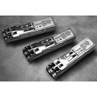
TXRX MM SFP LC CONN BAIL DELATCH
Manufacturer
Avago Technologies US Inc.
Series
-r
Specifications of HFBR-57E0PZ
Applications
Ethernet
Mounting Type
SFP
Voltage - Supply
2.97 V ~ 3.63 V
Connector Type
LC Duplex
Wavelength
1300nm
Data Rate
155MBd
Supply Voltage
3.3V
Wavelength Typ
1300nm
Leaded Process Compatible
Yes
Optical Fiber Type
TX/RX
Optical Rise Time
3/2.2ns
Optical Fall Time
3/2.2ns
Jitter
0.1/0.14ns
Operating Temperature Classification
Commercial
Peak Wavelength
1308/1380nm
Package Type
SFP
Operating Supply Voltage (min)
2.97V
Operating Supply Voltage (typ)
3.3V
Operating Supply Voltage (max)
3.63V
Output Current
50mA
Operating Temp Range
0C to 70C
Mounting
Snap Fit To Panel
Pin Count
20
Product
Transceiver
Maximum Rise Time
3 ns, 2.2 ns
Maximum Fall Time
3 ns, 2.2 ns
Pulse Width Distortion
0.1 ns, 0.14 ns
Maximum Output Current
50 mA
Operating Supply Voltage
2.97 V to 3.63 V
Maximum Operating Temperature
+ 70 C
Minimum Operating Temperature
0 C
Package / Case
SFP-20
Function
SFF Pluggable Transceivers with LC connector for ATM, FDDI, Fast Ethernet and SONET OC-3/SDH STM-1
Lead Free Status / RoHS Status
Lead free / RoHS Compliant
For Use With
Multimode Glass
Lead Free Status / RoHS Status
Lead free / RoHS Compliant, Lead free / RoHS Compliant
Available stocks
Company
Part Number
Manufacturer
Quantity
Price
Company:

Part Number:
HFBR-57E0PZ
Manufacturer:
Avago Technologies
Quantity:
135


13b. This specification is intended to indicate the performance of the receiver section of the transceiver when Input Optical Power signal
14a. All conditions of Note 13a apply except that the measurement is made at the center of the symbol with no window time- width.
14b. All conditions of Note 13b apply except that the measurement is made at the center of the symbol with no window time-width.
15a. Systematic Jitter contributed by the receiver is defined as the combination of Duty Cycle Distortion and Data Dependent Jitter. Systematic
15b Duty Cycle Distortion contributed by the receiver is measured at the 50% threshold of the electrical output signal using an IDLE Line
15c. Data Dependent Jitter contributed by the receiver is specified with the FDDI DDJ test pattern described in the FDDI PMD Annex A.5. The
16a. Random Jitter contributed by the receiver is specified with a 155.52 MBd (77.5 MHz square- wave) input signal.
16b. Random Jitter contributed by the receiver is specified with an IDLE Line State, 125 MBd (62.5 MHz square-wave), input signal. The input
17. This value is measured during the transition from low to high levels of input optical power.
18. This value is measured during the transition from high to low levels of input optical power. At Loss of Signal assert, the receiver outputs
19. The Loss of Signal output shall be de-asserted within 100 µs after a step increase of the Input Optical Power.
20. Loss of Signal output shall be asserted within 350 µs after a step decrease in the Input Optical Power. At Loss of Signal Assert, the receiver
21. The HFBR-57E0 transceiver complies with the requirements for the trade-offs between center wavelength, spectral width, and rise/fall
15
• At the Beginning of Life (BOL)
• Over the specified operating temperature and voltage ranges
• Input symbol pattern is the FDDI test pattern defined in FDDI PMD Annex A.5 with 4B/5B NRZI encoded data that contains a duty cycle
• Receiver data window time-width is 2.13 ns or greater and centered at mid-symbol. This worst case window time-width is the minimum
• Transmitter operating with an IDLE Line State pattern, 125 MBd (62.5 MHz square-wave), input signal to simulate any cross-talk present
characteristics are present per the following definitions. The Input Optical Power dynamic range from the minimum level (with a window
time-width) to the maximum level is the range over which the receiver is guaranteed to provide output data with a Bit Error Rate (BER)
better than or equal to 2.5 x 10
To test a receiver with the worst case FDDI PMD Active Input jitter condition requires exacting control over DCD, DDJ and RJ jitter
components that is difficult to implement with production test equipment. The receiver can be equivalently tested to the worst case
FDDI PMD input jitter conditions and meet the minimum output data window time-width of 2.13 ns. This is accomplished by using a nearly
ideal input optical signal (no DCD, insignificant DDJ and RJ) and measuring for a wider window time-width of 4.6 ns. This is possible due to
the cumulative effect of jitter components through their superposition (DCD and DDJ are directly additive and RJ components are rms
additive). Specifically, when a nearly ideal input optical test signal is used and the maximum receiver peak-to-peak jitter contributions of
DCD (0.4 ns), DDJ (1.0 ns), and RJ (2.14 ns) exist, the minimum window time-width becomes 8.0 ns -0.4 ns - 1.0 ns - 2.14 ns = 4.46 ns, or
conservatively 4.6 ns. This wider window time-width of 4.6 ns guarantees the FDDI PMD Annex E minimum window time-width of 2.13 ns
under worst case input jitter conditions to the Avago receiver.
Jitter is measured at 50% threshold using a 155.52 MBd (77.5 MHz square- wave), 2
State, 125 MBd (62.5 MHz square-wave), input signal. The input optical power level is -20 dBm average.
input optical power level is -20 dBm average.
optical power level is at maximum “P
Data Out and Data Out Bar go to steady PECL levels High and Low respectively.
outputs Data Out and Data Out Bar go to steady PECL levels High and Low respectively.
times shown in Figure 3. This figure is derived from the FDDI PMD standard (ISO/IEC 9314-3 : 1990 and ANSI X3.166 - 1990) per the
description in ANSI T1E1.2 Revision 3. The interpretation of this figure is that values of Center Wavelength and Spectral Width must lie
along the appropriate Optical Rise/Fall Time curve.
base-line wander effect of 50 kHz. This sequence causes a near worst case condition for inter-symbol interference.
allowed eye-opening presented to the FDDI PHY PM_Data indication input (PHY input) per the example in FDDI PMD Annex E. This
minimum window time-width of 2.13 ns is based upon the worst case FDDI PMD Active Input Interface optical conditions for peak-to-
peak DCD (1.0 ns), DDJ (1.2 ns) and RJ (0.76 ns) presented to the receiver.
between the transmitter and receiver sections of the transceiver.
-10
.
IN MIN
(W)”. See Application Information - Transceiver Jitter Section for further information.
23
-1 psuedorandom data pattern input signal.
Related parts for HFBR-57E0PZ
Image
Part Number
Description
Manufacturer
Datasheet
Request
R

Part Number:
Description:
XMITTER OPTICAL 2MBD SERCOS
Manufacturer:
Avago Technologies US Inc.
Datasheet:
Part Number:
Description:
Fiber Optic Transmitters, Receivers, Transceivers SERCOS TRANSMITTER
Manufacturer:
Avago Technologies US Inc.

Part Number:
Description:
RECEIVER FIBER OPTIC 600NM 40KBD
Manufacturer:
Avago Technologies US Inc.
Datasheet:

Part Number:
Description:
XMITTER FIBER OPTIC 600NM 5MBD
Manufacturer:
Avago Technologies US Inc.
Datasheet:

Part Number:
Description:
XMITTER FIBER OPTIC 600NM 40KBD
Manufacturer:
Avago Technologies US Inc.
Datasheet:

Part Number:
Description:
XMITTER VERSATILE LINK HORZ
Manufacturer:
Avago Technologies US Inc.
Datasheet:

Part Number:
Description:
XMITTER OPT HI PERFORMANCE VERT
Manufacturer:
Avago Technologies US Inc.
Datasheet:

Part Number:
Description:
TXRX FIBER OPTIC 650NM 10MBAUD
Manufacturer:
Avago Technologies US Inc.
Datasheet:
Part Number:
Description:
TXRX FIBER OPTIC 650NM 10MBAUD
Manufacturer:
Avago Technologies US Inc.
Datasheet:

Part Number:
Description:
FIBER OPTIC TRANSMITTER 660NM
Manufacturer:
Avago Technologies US Inc.
Datasheet:

Part Number:
Description:
KIT EVAL FIBER OPTIC 5MBD
Manufacturer:
Avago Technologies US Inc.
Datasheet:
Part Number:
Description:
KIT EVAL FIBER OPTICS 32MBD
Manufacturer:
Avago Technologies US Inc.
Datasheet:

Part Number:
Description:
KIT EVAL FIBER OPTIC 5MBD
Manufacturer:
Avago Technologies US Inc.
Datasheet:

Part Number:
Description:
125MBd 1300nm FiberOptic Eval Kit
Manufacturer:
Avago Technologies US Inc.
Datasheet:

Part Number:
Description:
DC-5MBd 820nm FiberOptic EvalKit
Manufacturer:
Avago Technologies US Inc.
Datasheet: