AFCT-5611Z Avago Technologies US Inc., AFCT-5611Z Datasheet - Page 12
AFCT-5611Z
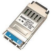
Manufacturer Part Number
AFCT-5611Z
Description
TXRX 1.25GBD GBIC PLUGGABLE
Manufacturer
Avago Technologies US Inc.
Datasheet
1.AFBR-5601Z.pdf
(13 pages)
Specifications of AFCT-5611Z
Applications
Ethernet
Data Rate
1.25Gbd
Wavelength
1310nm
Voltage - Supply
4.75 V ~ 5.25 V
Connector Type
GBIC
Mounting Type
Panel Mount
Supply Voltage
5V
Wavelength Typ
850nm
Peak Reflow Compatible (260 C)
Yes
Leaded Process Compatible
Yes
Optical Fiber Type
TX/RX
Optical Rise Time
0.26/0.35ns
Optical Fall Time
0.26/0.35ns
Jitter
0.227ns
Operating Temperature Classification
Commercial
Peak Wavelength
860nm
Operating Supply Voltage (min)
4.75V
Operating Supply Voltage (typ)
5V
Operating Supply Voltage (max)
5.25V
Operating Temp Range
0C to 60C
Pin Count
20
Lead Free Status / RoHS Status
Lead free / RoHS Compliant
Lead Free Status / RoHS Status
Lead free / RoHS Compliant, Lead free / RoHS Compliant


Transceiver Electrical Characteristics
(T
AFCT-5611Z
Transmitter Electrical Characteristics
(T
Receiver Electrical Characteristics
(T
Notes:
1. Pull-up resistor on host V
2. Rising edge of TX_DISABLE to fall of output signal below 10% of nominal.
3. Falling edge of TX_DISABLE to rise of output signal above 90% of nominal.
4. From power on or hot plug after V
5. From occurrence of fault (output safety violation or V
6. TX_DISABLE HIGH before TX_DISABLE set LOW.
7. 20 - 80% values.
Notes:
1. See Figure 1 for measurement point.
2. Maximum current is specified at V
3. Hot plug above actual steady state current.
4. Total T
12
Parameter
Surge Current
Power Dissipation
Parameter
Transmitter Differential Input Voltage
Tranmit Fault Load
Transmit Fault Output - Low
Transmit Fault Output - High
TX_DISABLE Assert Time
TX_DISABLE Negate Time
Time to initialize, includes reset of
TX_FAULT
TX_FAULT from fault to assertion
TX_DISABLE time to start reset
Parameter
Receiver Differential Output Voltage
Receiver Output Rise Time
Receiver Output Fall Time
Receiver Loss of Light Load
Receiver Loss of Signal
Output Voltage - Low
Receiver Loss of Signal
Output Voltage - High
Receiver Loss of Signal
Assert Time (off to on)
Receiver Loss of Signal
Deassert Time (on to off )
A
A
A
= 0°C to +60°C, V
= 0°C to +60°C, V
= 0°C to +60°C, V
X
+ R
X
.
CC
CC
CC
CC
= 4.75 V to 5.25 V)
= 4.75 V to 5.25 V)
= 4.75 V to 5.25 V)
.
CC
DD
= maximum @ maximum operating temperature and end of life.
T >4.75 V or From negation of TX_DISABLE during reset of TX_FAULT.
Symbol
I
P
Symbol
±TX_DAT
TX_FAULT
TX_FAULT
TX_FAULT
t_off
t_on
t_init
t_fault
t_reset
Symbol
±RX_DAT
t
t
RX_LOS
RX_LOS
RX_LOS
t
t
SURGE
rRX_DAT
fRX_DAT
A,RX_LOS
D,RX_LOS
DISS
DD
Load
L
H
T <4.5 V).
Load
L
H
Min.
Min.
650
4.7
0.0
V
10
Min.
370
4.7
0.0
V
CC
CC
-0.5
-0.5
Typ.
1.00
Typ.
3
0.5
30
20
Typ.
Max.
+30
1.58
Max.
2000
10
0.5
V
10
1
300
100
Max.
2000
0.35
0.35
10
0.5
V
100
100
CC
CC
+0.3
+0.3
Unit
mA
W
Unit
mV p-p
kW
v
v
µsec
msec
msec
µsec
µsec
Unit
mV p-p
ns
ns
kW
V
V
µs
µs
Notes
3
4
Notes
1
2
3
4
5
6
Notes
7
7
1
Related parts for AFCT-5611Z
Image
Part Number
Description
Manufacturer
Datasheet
Request
R

Part Number:
Description:
TXRX OPT 1X9 155MB/S 1300NM BK
Manufacturer:
Avago Technologies US Inc.
Datasheet:

Part Number:
Description:
TXRX OPT SFF PLUGGABLE BAIL
Manufacturer:
Avago Technologies US Inc.
Datasheet:
Part Number:
Description:
TXRX OPT SFF PLUGGABLE BAIL DMI
Manufacturer:
Avago Technologies US Inc.
Datasheet:

Part Number:
Description:
TXRX 125MBD DUPLEX BLACK SC 1X9
Manufacturer:
Avago Technologies US Inc.
Datasheet:
Part Number:
Description:
TXRX 125MBD DUPLEX BLUE SC 1X9
Manufacturer:
Avago Technologies US Inc.
Datasheet:

Part Number:
Description:
TXRX OPT SM 155MBS SONET OC3/SDH
Manufacturer:
Avago Technologies US Inc.
Datasheet:
Part Number:
Description:
TXRX SFF SM OC3/STM-1 BAIL DMI
Manufacturer:
Avago Technologies US Inc.
Datasheet:
Part Number:
Description:
TXRX 125MBD DUPLEX BLACK SC 1X9
Manufacturer:
Avago Technologies US Inc.
Datasheet:
Part Number:
Description:
TXRX 125MBD DUPLEX BLUE SC 1X9
Manufacturer:
Avago Technologies US Inc.
Datasheet:

Part Number:
Description:
TXRX OPT SM 155MBS SONET OC3/SDH
Manufacturer:
Avago Technologies US Inc.
Datasheet:

Part Number:
Description:
OPTOCOUPLER GATE DRV 2A 16-SOIC
Manufacturer:
Avago Technologies US Inc.
Datasheet:
Part Number:
Description:
OPTOCOUPLER 2CH 2.5A 16-SOIC
Manufacturer:
Avago Technologies US Inc.
Datasheet:

Part Number:
Description:
OPTOCOUPLER GATE DRV 0.4A 16SOIC
Manufacturer:
Avago Technologies US Inc.
Datasheet:

Part Number:
Description:
OPTOCOUPLER 2.0A 250KHZ 8-DIP
Manufacturer:
Avago Technologies US Inc.
Datasheet:

Part Number:
Description:
OPTOCOUPLER 2.0A 250KHZ GW 8-SMD
Manufacturer:
Avago Technologies US Inc.
Datasheet: