HFBR-1515BZ Avago Technologies US Inc., HFBR-1515BZ Datasheet - Page 6
HFBR-1515BZ
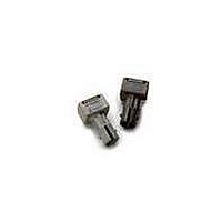
Manufacturer Part Number
HFBR-1515BZ
Description
XMITTER FIBER OPTIC PROFIBUS ST
Manufacturer
Avago Technologies US Inc.
Datasheet
1.HFBR-2505AZ.pdf
(11 pages)
Specifications of HFBR-1515BZ
Wavelength
650nm
Spectral Bandwidth
21nm
Voltage - Forward (vf) Typ
2.1V
Current - Dc Forward (if)
60mA
Voltage - Dc Reverse (vr) (max)
3V
Capacitance
60pF
Connector Type
ST
Function
Fiber Optic Transmitter for PROFBUS, ST Port
Product
Transmitter
Data Rate
10 MBd
Diode Capacitance
60 pF
Maximum Rise Time
13 ns
Maximum Fall Time
10 ns (Typ)
Operating Supply Voltage
5.5 VDC
Maximum Operating Temperature
+ 85 C
Minimum Operating Temperature
- 40 C
Package / Case
PDIP-6
Lead Free Status / RoHS Status
Lead free / RoHS Compliant
For Use With
Plastic Optical Fiber, Hard Clad Silica
Lead Free Status / RoHS Status
Lead free / RoHS Compliant, Lead free / RoHS Compliant


HFBR-25x5AZ/BZ Receivers
The HFBR-25x5AZ/BZ receiver consists of a silicon PIN
photodiode and digitizing IC to produce a logic compat-
ible output. The IC includes a unique circuit to correct
the pulse width distortion of the first bit after a long idle
period. This enables operation from DC to 10 MBd with
low PWD for arbitrary data patterns. The receiver output is
a “push–pull” stage compatible with TTL and CMOS logic.
The receiver housing is a dark grey, conductive plastic.
The HFBR-2505AZ is compatible with SMA connectors,
while the HFBR-2515BZ mates with ST
Absolute Maximum Ratings
Electrical/Optical Characteristics
-0°C to +70°C, 4.75 V < V
Parameter
Peak Input Power Level
Logic HIGH
Peak Input Power Level
Logic LOW
Supply Current
High Level Output
Voltage
Low Level Output Voltage
Output Rise Time
Output Fall Time
Notes:
1. Typical data are at 25˚C, V
2. 1.6 mm below seating plane.
3. In recommended receiver circuit, with an optical signal from the recommended transmitter circuit.
4. Pins 1 and 4 are electrically connected to the conductive housing and are also used for mounting and retaining purposes. It is required that
5. BER ≤10E-9, includes a 10.8 dB margin below the receiver switching threshold level (signal to noise ratio = 12).
6
Parameter
Storage and Operating Temperature
Supply Voltage
Average Output Current
Output Power Dissipation
Lead Soldering Cycle
pin 1 and 4 be connected to ground to maintain conductive housing shield effectiveness.
CC
CC
= 5.0 V.
< 5.25 V, V
Symbol
Temp
Time
V
V
P
P
I
CC
t
t
RH
OH
OH
RL
r
f
P–P
®
connectors.
Noise ≤ 100 mV unless otherwise noted
Min.
–20
–22
4.2
Symbol
I
O,AVG
P
V
T
OD
CC
S
Typ.
0.22
4.7
27
12
10
[1]
Min.
–0.5
–40
–16
Max.
–42
–44
0.4
–0
–2
45
30
30
Max.
+5.5
+16
260
85
80
10
dBm
dBm
Unit
mA
PIN
ns
ns
V
V
1
4
5
6
7
8
BOTTOM VIEW,
HFBR 25x5AZ/BZ
SEE NOTE 4
CONNECTED TO PIN 4
CONNECTED TO PIN 1
NO CONNECT
V
GND
V
4
1
CC
O
5
6
7
8
FUNCTION
Condition
1 mm POF
200 µm HCS
1 mm POF,
200 µm HCS
|PWD| < 30 ns
V
I
I
C
CL = 10 pF
O
O
Unit
mW
O
mA
L
°C
˚C
= –40 µA
= +1.6 mA
V
s
= 10 pF
= Open
®
®
Reference
Note 2
Ref.
Notes 3, 5
Note 3
Figs. 7, 8,
9, 10
Note 3
Note 3
Related parts for HFBR-1515BZ
Image
Part Number
Description
Manufacturer
Datasheet
Request
R

Part Number:
Description:
XMITTER FIBER OPTIC SERCOS SMA
Manufacturer:
Avago Technologies US Inc.
Datasheet:

Part Number:
Description:
FIBER OPTIC CBL SIMPLEX 1=100M
Manufacturer:
Avago Technologies US Inc.
Datasheet:

Part Number:
Description:
FIBER OPTIC CBL SIMPLEX 1=500M
Manufacturer:
Avago Technologies US Inc.
Datasheet:

Part Number:
Description:
FIBER OPTIC CONN LATCH GRY SIMPL
Manufacturer:
Avago Technologies US Inc.
Datasheet:

Part Number:
Description:
FIBER OPTIC CONN LATCH BLU SIMPL
Manufacturer:
Avago Technologies US Inc.
Datasheet:

Part Number:
Description:
XMITTER VERSATILE LINK HORZ
Manufacturer:
Avago Technologies US Inc.
Datasheet:

Part Number:
Description:
Fiber Optic Transmitters, Receivers, Transceivers 1300nm 155MBd 16-pin DIP ST Rx
Manufacturer:
Avago Technologies US Inc.

Part Number:
Description:
FIBER OPTIC CBL DUPLEX 1=100M
Manufacturer:
Avago Technologies US Inc.
Datasheet:
Part Number:
Description:
FIBER OPTIC CBL SIMPLEX 1=500M
Manufacturer:
Avago Technologies US Inc.
Datasheet:
Part Number:
Description:
FIBER OPTIC CBL DUPLEX 1=500M
Manufacturer:
Avago Technologies US Inc.
Datasheet:

Part Number:
Description:
OPTOCOUPLER GATE DRV 2A 16-SOIC
Manufacturer:
Avago Technologies US Inc.
Datasheet:
Part Number:
Description:
OPTOCOUPLER 2CH 2.5A 16-SOIC
Manufacturer:
Avago Technologies US Inc.
Datasheet:

Part Number:
Description:
OPTOCOUPLER GATE DRV 0.4A 16SOIC
Manufacturer:
Avago Technologies US Inc.
Datasheet:

Part Number:
Description:
OPTOCOUPLER 2.0A 250KHZ 8-DIP
Manufacturer:
Avago Technologies US Inc.
Datasheet:

Part Number:
Description:
OPTOCOUPLER 2.0A 250KHZ GW 8-SMD
Manufacturer:
Avago Technologies US Inc.
Datasheet: