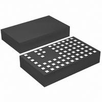
LTM4604IV#PBF Linear Technology, LTM4604IV#PBF Datasheet - Page 15

LTM4604IV#PBF
Manufacturer Part Number
LTM4604IV#PBF
Description
IC DC/DC UMODULE 4A 66-LGA
Manufacturer
Linear Technology
Series
µModuler
Type
Point of Load (POL) Non-Isolatedr
Datasheet
1.LTM4604EVPBF.pdf
(20 pages)
Specifications of LTM4604IV#PBF
Design Resources
LTM4604 Spice Model
Output
0.8 ~ 5 V
Number Of Outputs
1
Power (watts)
20W
Mounting Type
Surface Mount
Voltage - Input
2.38 ~ 5.5 V
Package / Case
66-LGA
1st Output
0.8 ~ 5 VDC @ 4A
Size / Dimension
0.59" L x 0.35" W x 0.09" H (15mm x 9mm x 2.3mm)
Power (watts) - Rated
20W
Operating Temperature
-40°C ~ 85°C
Lead Free Status / RoHS Status
Lead free / RoHS Compliant
3rd Output
-
2nd Output
-
Available stocks
Company
Part Number
Manufacturer
Quantity
Price
Safety Considerations
The LTM4604 modules do not provide isolation from V
V
with a rating twice the maximum input current needs to be
provided to protect each unit from catastrophic failure.
Layout Checklist/Example
The high integration of LTM4604 makes the PCB board
layout very simple and easy. However, to optimize its electri-
cal and thermal performance, some layout considerations
are still necessary.
APPLICATIONS INFORMATION
• Use large PCB copper areas for high current path,
• Place high frequency ceramic input and output capacitors
• Place a dedicated power ground layer underneath the
• To minimize the via conduction loss and reduce module
OUT
including V
PCB conduction loss and thermal stress.
next to the V
frequency noise.
unit.
thermal stress, use multiple vias for interconnection
between top layer and other power layers.
. There is no internal fuse. If required, a slow blow fuse
IN
, GND and V
IN
, GND and V
OUT
OUT
. It helps to minimize the
Figure 15. Typical 2.375V to 5.5V Input, 1.5V at 4A Design
pins to minimize high
OPEN-DRAIN
C
0.01μF
SSEXT
PULL UP
X5R OR X7R
10μF
6.3V
C
IN
PGOOD
COMP
RUN/SS
2.375V TO 5.5V
LTM4604
IN
GND
V
V
IN
IN
to
TRACK
V
OUT
FB
Figure 14 gives a good example of the recommended
layout. For easier PC board layout and assembly due
to increased spacing between land grid pads, please
refer to the LTM4604A.
• Do not put vias directly on the pads unless they are
• SW pads can be soldered to board to improve thermal
capped.
performance.
R
5.69k
0.5%
FB
V
4604 F15
IN
Figure 14. Recommended PCB Layout
C
22μF 3
6.3V
X5R OR X7R
REFER TO
TABLE 4
OUT
C
IN
•
•
V
1.5V
4A
OUT
•
•
•
•
•
•
•
•
•
•
•
•
•
•
•
•
GND
•
•
•
•
•
•
•
SW
•
•
•
•
•
•
•
•
•
•
•
V
OUT
•
•
•
•
C
C
C
OUT
OUT
OUT
•
•
•
LTM4604
•
•
•
•
•
•
•
•
•
•
•
•
•
•
•
•
GND
•
•
•
•
•
4604 F14
•
•
•
15
4604fa


