P0001 Terasic Technologies Inc, P0001 Datasheet
P0001
Specifications of P0001
Available stocks


Related parts for P0001


P0001 Summary of contents
Page 1
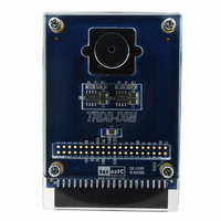
Terasic TRDB_D5M Digital Camera Package TRDB_D5M 5 Mega Pixel Digital Camera Development Kit Document Version 1.2 AUG. 10, 2010 by Terasic ...
Page 2
Terasic TRDB_D5M Page Index CHAPTER 1 ABOUT THE KIT................................................................................................................................. 1 1 ..................................................................................................................................................... 1 IT ONTENTS 1 ...................................................................................................................................... 2 SSEMBLE THE AMERA 1 ..................................................................................................................................................... 4 ETTING ELP CHAPTER 2 TRDB_D5M.......................................................................................................................................... 5 2.1 F ............................................................................................................................................................. 5 ...
Page 3
Chapter The TRDB_D5M Kit provides everything you need to develop a 5 Mega Pixel Digital Camera on the Altera DE4 / DE2_115 / DE2-70 / DE2 / DE1 boards. The kit contains hardware design (in Verilog) and software to ...
Page 4
Assemble the Camera 1.2 Please follow the step below to assemble your camera: 1. Connect the D5M to your DE4 board as shown in Figure 1.2. Figure 1.2 Connect the D5M to DE4 board’s expansion port (outermost port). 2. Connect ...
Page 5
Connect the D5M to your DE2 board as shown in Figure 1.5. Figure 1.5 Connect the D5M to DE2 board’s expansion port (outermost port). 5. Connect the D5M to your DE1 board as shown in Figure 1.6. Figure 1.6 ...
Page 6
Getting Help 1.3 Here are some places to get help if you encounter any problem: Email to support@terasic.com Taiwan & China: +886-3-550-8800 Korea : +82-2-512-7661 Japan: +81-428-77-7000 English Support Line: +1-408-512-1336 4 Digital Camera Design Demonstration ...
Page 7
Chapter This chapter will illustrate the technical details users need to know to modify the reference design for their own purpose. The D5M kit is designed to use the same strict design and layout practices used in high-end consumer ...
Page 8
Key Performance Parameters Maximum data rate/master clock Frame rate Supply Voltage Note. For detail specification of D5M, please refer to TRDB-D5M_Hardware specification.PDF Parameter Active pixels 2,592H x 1,944V Pixel size 2.2μ 2.2μ m Color filter array RGB Bayer ...
Page 9
Pin-out of the 40-pin connector on TRDB-D5M 2.2 PIXCLK XCLKIN STROBE 23 FVAL 25 SCLK 27 VCC33 ...
Page 10
Pin Description of the 40-pin Interface of TRDB_D5M 2.3 The TRDB_D5M has a 40-pin connector on the board. The pin description of the 40-pin connector follows: Pin Numbers ...
Page 11
Chapter Digital Camera Design This chapter illustrates how to exercise the digital camera reference design provided with the kit. Users can follow the instructions in this chapter to build a 5 Mega Pixel camera using their DE4 / DE2_115 ...
Page 12
Camera Demonstration Setup On DE4 Board 3.2 Locate the project directory from the CD-ROM included and follow the steps below: Directory: Demonstration / DE4_230/530_D5M_DVI FPGA Bitstream Used: DE4_230/530_ D5M_DVI.sof 1. Ensure the connection is made correctly as shown in Figure ...
Page 13
Figure 3.2. The Connection Setup for DE4 users Table 3.1 The functional keys of the digital camera demonstration Component BUTTON [0] BUTTON [1] BUTTON [2] BUTTON [3] SLIDE_SW [0] SLIDE_SW [16] SW [0] HEX[1:0] 12. User can revise the header ...
Page 14
Camera Demonstration Setup On DE2-115 Board 3.3 Locate the project directory from the CD-ROM included and follow the steps below: Directory: Demonstration / DE2_115_CAMERA FPGA Bitstream Used: DE2_115_ CAMERA.sof 1. Ensure the GPIO voltage level is set to 3.3V via ...
Page 15
User can revise the header file "VGA_Param.h" in the project to select the system resolution between SVGA@800*600 and VGA@640*480. 12. After revision, regenerate the project and repeat above steps. Configuring the Camera and Load the Image Captured to 3.4 ...
Page 16
Your PC (DE2-70 Board Users) Locate the project directory from the CD-ROM included and follow the steps below: Directory: Demonstration / DE2_70_CAMERA / SW FPGA Bitstream Used: DE2_70_ CAMERA.sof 1. Ensure the connection is made correctly as shown in Figure ...
Page 17
Figure 3.4. The Connection Setup for DE2-70 users Table 3.3 The functional keys of the digital camera demonstration Component KEY[0] KEY[1] KEY[2] KEY[3] SW[0] SW[16] HEX[7:0] 12. Users can upload the captured image clicking the ‘Capture’ button ...
Page 18
Digital Camera Design Demonstration Figure 3.5. The DE2_70_camera tool 16 ...
Page 19
Configuring the Camera (DE2 Board Users) 3.5 Locate the project directory from the CD-ROM included and follow the steps below: Directory: Demonstration / DE2_CAMERA FPGA Bitstream Used: DE2_D5M.sof or DE2_D5M.pof 1. Ensure the connection is set correctly as shown in ...
Page 20
Table 3.4 The functional keys of the digital camera demonstration Component KEY[0] Reset circuit KEY[1] Set the new exposure time (use with SW[0] ) KEY[2] Trigger the Image Capture (take a shot) KEY[3] Switch to Free Run mode Off: Extend ...
Page 21
Configuring the Camera (DE1 Board Users) 3.6 Locate the project directory from the CD-ROM included and follow the steps below: Directory: Demonstration / DE1_CAMERA FPGA Bitstream Used: DE1_D5M.sof or DE1_D5M.pof 1. Ensure the connection is set correctly as shown in ...
Page 22
Table 3.5 The functional keys of the digital camera demonstration Component KEY[0] Reset circuit KEY[1] Set the new exposure time (use with SW[0] ) KEY[2] Trigger the Image Capture (take a shot) KEY[3] Switch to Free Run mode Off: Extend ...
Page 23
Block Diagram of the Reference Design 3.7 The complete reference design is also located in the CD-ROM attached. Please refer to the following diagram to help you in reading the code provided. DATA FVAL LVAL CMOS Sensor Data Capture PCLK ...
Page 24
Chapter Date MAR, 24, 2008 AUG, 03, 2009 AUG, 10, 2010 Always Visit TRDB_D5M Webpage for New Applications 4.2 We will be continuing providing interesting examples and labs on our TRDB_D5M webpage. Please visit Digital Camera Design Demonstration Chapter ...