P0528 Terasic Technologies Inc, P0528 Datasheet
P0528
Specifications of P0528


Related parts for P0528


P0528 Summary of contents
Page 1
Altera DE1 Board DE1 Development and Education Board Version 1.1 User Manual Copyright © 2006 Altera Corporation ...
Page 2
Altera DE1 Board CONTENTS Chapter 1 DE1 Package.....................................................................................................................1 1.1 Package Contents .................................................................................................................1 1.2 The DE1 Board Assembly....................................................................................................2 1.3 Getting Help.........................................................................................................................3 Chapter 2 Altera DE1 Board.............................................................................................................4 2.1 Layout and Components ......................................................................................................4 2.2 Block Diagram of the DE1 Board........................................................................................6 2.3 Power-up the ...
Page 3
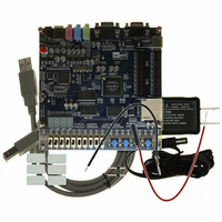
The DE1 package contains all components needed to use the DE1 board in conjunction with a computer that runs the Microsoft Windows software. 1.1 Package Contents Figure 1.1 shows a photograph of the DE1 package. The DE1 package includes: • ...
Page 4
CD-ROMs containing Altera’s Quartus embedded processor • Bag of six rubber (silicon) covers for the DE1 board stands. The bag also contains some extender pins, which can be used to facilitate easier probing with testing equipment of the board’s ...
Page 5
Getting Help Here are the addresses where you can get help if you encounter problems: • Altera Corporation 101 Innovation Drive San Jose, California, 95134 USA Email: university@altera.com • Terasic Technologies No. 356, Sec. 1, Fusing E. Rd. Jhubei ...
Page 6
Altera DE1 Board This chapter presents the features and design characteristics of the DE1 board. 2.1 Layout and Components A photograph of the DE1 board is shown in Figure 2.1. It depicts the layout of the board and indicates the ...
Page 7
The following hardware is provided on the DE1 board: • Altera Cyclone ® II 2C20 FPGA device • Altera Serial Configuration device – EPCS4 • USB Blaster (on board) for programming and user API control; both JTAG and Active Serial ...
Page 8
Block Diagram of the DE1 Board Figure 2.2 gives the block diagram of the DE1 board. To provide maximum flexibility for the user, all connections are made through the Cyclone II FPGA device. Thus, the user can configure the ...
Page 9
Static RAM memory chip • Organized as 256K x 16 bits • Accessible as memory for the Nios II processor and by the DE1 Control Panel SDRAM • 8-Mbyte Single Data Rate Synchronous Dynamic RAM memory chip • ...
Page 10
Applications for MP3 players and recorders, PDAs, smart phones, voice recorders, etc. VGA output • Uses a 4-bit resistor-network DAC • With 15-pin high-density D-sub connector • Supports up to 640x480 at 60-Hz refresh rate • Can be used ...
Page 11
All user LEDs are flashing • All 7-segment displays are cycling through the numbers • The VGA monitor displays the image shown in Figure 2.3 and Figure2.4 according to SW0. • Set the toggle switch SW9 ...
Page 12
DE1 Control Panel The DE1 board comes with a Control Panel facility that allows a user to access various components on the board through a USB connection from a host computer. This chapter first presents some basic functions of the ...
Page 13
The Control Panel is now ready for use; experiment by setting the value of some 7-segment display and observing the result on the DE1 board. Figure 3.1. Quartus II Programmer window. The concept of the DE1 Control Panel is ...
Page 14
The provided IP handles all requests and performs data transfers between the computer and the DE1 board. Figure 3.3. The DE1 Control Panel concept. The DE1 Control Panel can be used to change the ...
Page 15
Figure 3.4. Controlling LEDs and the LCD display. 3.3 SDRAM/SRAM Controller and Programmer The Control Panel can be used to write/read data to/from the SDRAM and SRAM chips on the DE1 board. We will describe how the SDRAM may be ...
Page 16
A 16-bit word can be written into the SDRAM by entering the address of the desired location, specifying the data to be written, and pressing the Write button. Contents of the location can be read by pressing the Read button. ...
Page 17
Read one byte from the memory • Write a binary file to the memory • Load the contents of the Flash memory into a file Note the following characteristics of the Flash memory: • The Flash memory chip is ...
Page 18
To read a byte of data from a random location, enter the address of the location and click on the Read button. The rDATA box will display the data read back from the address specified. The Sequential Write function is ...
Page 19
To let users implement and test their IP cores (written in Verilog) without requiring them to implement complex API/Host control software and memory (SRAM/SDRAM/Flash) controllers, we provide an integrated control environment consisting of a software controller in C++, a USB ...
Page 20
TOOLS – Multi-Port SRAM/SDRAM/Flash Controller The TOOLS page of the Control Panel GUI allows selection of the User Ports. We will illustrate a typical process by implementing a Flash Music Player. The music data is loaded into the Flash ...
Page 21
Audio DAC circuit. 6. Note that the Asynchronous Port 1 is connected to the Audio DAC part, as shown in Figure 3.7. Once you selected Asynchronous Port 1 and clicked the Configure button, the Audio DAC Controller ...
Page 22
The image in Figure 3.9 is stored in an M4K memory block in the Cyclone II FPGA loaded into the M4K block in the MIF/Hex(Intel) format during the default bit stream configuration stage. We will next describe how ...
Page 23
Figure 3.11. Multi-Port Controller configured to display an image from the SRAM. Figure 3.12. A displayed image. 21 DE1 User Manual ...
Page 24
You can display any image file by loading it into the SRAM chip or into an M4K memory block in the Cyclone II chip. This requires generating a bitmap file, which may be done as follows: 1. Load the desired ...
Page 25
Image Source R/G/B Band Filter Color Picture R/G/B Color Picture R/G/B (optional) Grayscale N/A Picture Grayscale N/A Picture Note: Raw_Data_BW.txt is used to fill in the MIF/Intel Hex format for M4K SRAM B&W Output Result Threshold (640x480) Filter N/A Raw_Data_Gray ...
Page 26
Using the DE1 Board This chapter gives instructions for using the DE1 board and describes each of its I/O devices. 4.1 Configuring the Cyclone II FPGA The procedure for downloading a circuit from a host computer to the DE1 board ...
Page 27
Figure 4.1 illustrates the JTAG configuration setup. To download a configuration bit stream into the Cyclone II FPGA, perform the following steps: • Ensure that power is applied to the DE1 board • Connect the supplied USB cable to the ...
Page 28
USB Blaster Circuit USB Quartus II MAX Programmer 3128 AS Mode Figure 4.2. The AS configuration scheme. In addition to its use for JTAG and AS programming, the USB Blaster port on the DE1 board can also be used to ...
Page 29
There are 27 user-controllable LEDs on the DE1 board. Eighteen red LEDs are situated above the 18 toggle switches, and eight green LEDs are found above the pushbutton switches (the 9 LED is in the middle of the 7-segment displays). ...
Page 30
Figure 4.5. Schematic diagram of the LEDs. Signal Name FPGA Pin No. SW[0] PIN_L22 SW[1] PIN_L21 SW[2] PIN_M22 SW[3] PIN_V12 SW[4] PIN_W12 SW[5] PIN_U12 SW[6] PIN_U11 SW[7] PIN_M2 Description Toggle Switch[0] Toggle Switch[1] Toggle Switch[2] Toggle Switch[3] Toggle Switch[4] Toggle ...
Page 31
SW[8] PIN_M1 SW[9] PIN_L2 Table 4.1. Pin assignments for the toggle switches. Signal Name FPGA Pin No. KEY[0] PIN_R22 KEY[1] PIN_R21 KEY[2] PIN_T22 KEY[3] PIN_T21 Table 4.2. Pin assignments for the pushbutton switches. Signal Name FPGA Pin No. LEDR[0] PIN_R20 ...
Page 32
Using the 7-segment Displays The DE1 Board has four 7-segment displays. These displays are arranged into a group of four, with the intent of displaying numbers of various sizes. As indicated in the schematic in Figure 4.6, the seven ...
Page 33
Signal Name HEX0[0] HEX0[1] HEX0[2] HEX0[3] HEX0[4] HEX0[5] HEX0[6] HEX1[0] HEX1[1] HEX1[2] HEX1[3] HEX1[4] HEX1[5] HEX1[6] HEX2[0] HEX2[1] HEX2[2] HEX2[3] HEX2[4] HEX2[5] HEX2[6] HEX3[0] HEX3[1] HEX3[2] HEX3[3] HEX3[4] HEX3[5] HEX3[6] Table 4.4. Pin assignments for the 7-segment displays. 4.4 Clock ...
Page 34
Figure 4.8. Schematic diagram of the clock circuit. Signal Name CLOCK_27 CLOCK_50 CLOCK_24 EXT_CLOCK Table 4.5. Pin assignments for the clock inputs. 4.5 Using the Expansion Header The DE1 Board provides two 40-pin expansion headers. Each header connects directly to ...
Page 35
Figure 4.10. Schematic diagram of the expansion headers. Signal Name FPGA Pin No. GPIO_0[0] PIN_A13 Description GPIO Connection 0[0] 33 DE1 User Manual ...
Page 36
GPIO_0[1] PIN_B13 GPIO_0[2] PIN_A14 GPIO_0[3] PIN_B14 GPIO_0[4] PIN_A15 GPIO_0[5] PIN_B15 GPIO_0[6] PIN_A16 GPIO_0[7] PIN_B16 GPIO_0[8] PIN_A17 GPIO_0[9] PIN_B17 GPIO_0[10] PIN_A18 GPIO_0[11] PIN_B18 GPIO_0[12] PIN_A19 GPIO_0[13] PIN_B19 GPIO_0[14] PIN_A20 GPIO_0[15] PIN_B20 GPIO_0[16] PIN_C21 GPIO_0[17] PIN_C22 GPIO_0[18] PIN_D21 GPIO_0[19] PIN_D22 GPIO_0[20] PIN_E21 ...
Page 37
GPIO_1[2] PIN_H14 GPIO_1[3] PIN_G15 GPIO_1[4] PIN_E14 GPIO_1[5] PIN_E15 GPIO_1[6] PIN_F15 GPIO_1[7] PIN_G16 GPIO_1[8] PIN_F12 GPIO_1[9] PIN_F13 GPIO_1[10] PIN_C14 GPIO_1[11] PIN_D14 GPIO_1[12] PIN_D15 GPIO_1[13] PIN_D16 GPIO_1[14] PIN_C17 GPIO_1[15] PIN_C18 GPIO_1[16] PIN_C19 GPIO_1[17] PIN_C20 GPIO_1[18] PIN_D19 GPIO_1[19] PIN_D20 GPIO_1[20] PIN_E20 GPIO_1[21] PIN_F20 ...
Page 38
Using VGA The DE1 board includes a 16-pin D-SUB connector for VGA output. The VGA synchronization signals are provided directly from the Cyclone II FPGA, and a 4-bit DAC using resistor network is used to produce the analog data ...
Page 39
During the data display interval the RGB data drives each pixel in turn across the row being displayed. Finally, there is a time period called the front porch (d) where the RGB signals must again be off before the next ...
Page 40
VGA_B[0] VGA_B[1] VGA_B[2] VGA_B[3] VGA_HS VGA_VS 4.7 Using the 24-bit Audio CODEC The DE1 board provides high-quality 24-bit audio via the Wolfson WM8731 audio CODEC (enCOder/DECoder). This chip supports microphone-in, line-in, and line-out ports, with a sample rate adjustable from ...
Page 41
Signal Name AUD_ADCLRCK AUD_ADCDAT AUD_DACLRCK AUD_DACDAT AUD_XCK AUD_BCLK I2C_SCLK I2C_SDAT Table 4.9. Audio CODEC pin assignments. 4.8 RS-232 Serial Port The DE1 board uses the MAX232 transceiver chip and a 9-pin D-SUB connector for RS-232 communications. For detailed information on ...
Page 42
PS/2 Serial Port The DE1 board includes a standard PS/2 interface and a connector for a PS/2 keyboard or mouse. Figure 4.17 shows the schematic of the PS/2 circuit. Instructions for using a PS/2 mouse or keyboard can be ...
Page 43
Figure 4.23. SDRAM schematic. Figure 4.24. SRAM schematic. 41 DE1 User Manual ...
Page 44
Figure 4.25. Flash schematic. Signal Name FPGA Pin No. DRAM_ADDR[0] PIN_W4 DRAM_ADDR[1] PIN_W5 DRAM_ADDR[2] PIN_Y3 DRAM_ADDR[3] PIN_Y4 DRAM_ADDR[4] PIN_R6 DRAM_ADDR[5] PIN_R5 DRAM_ADDR[6] PIN_P6 DRAM_ADDR[7] PIN_P5 DRAM_ADDR[8] PIN_P3 DRAM_ADDR[9] PIN_N4 DRAM_ADDR[10] PIN_W3 DRAM_ADDR[11] PIN_N6 DRAM_DQ[0] PIN_U1 DRAM_DQ[1] PIN_U2 DRAM_DQ[2] PIN_V1 DRAM_DQ[3] ...
Page 45
DRAM_DQ[7] PIN_Y2 DRAM_DQ[8] PIN_N1 DRAM_DQ[9] PIN_N2 DRAM_DQ[10] PIN_P1 DRAM_DQ[11] PIN_P2 DRAM_DQ[12] PIN_R1 DRAM_DQ[13] PIN_R2 DRAM_DQ[14] PIN_T1 DRAM_DQ[15] PIN_T2 DRAM_BA_0 PIN_U3 DRAM_BA_1 PIN_V4 DRAM_LDQM PIN_R7 DRAM_UDQM PIN_M5 DRAM_RAS_N PIN_T5 DRAM_CAS_N PIN_T3 DRAM_CKE PIN_N3 DRAM_CLK PIN_U4 DRAM_WE_N PIN_R8 DRAM_CS_N PIN_T6 Table 4.16. ...
Page 46
SRAM_ADDR[14] PIN_R10 SRAM_ADDR[15] PIN_T7 SRAM_ADDR[16] PIN_Y6 SRAM_ADDR[17] PIN_Y5 SRAM_DQ[0] PIN_AA6 SRAM_DQ[1] PIN_AB6 SRAM_DQ[2] PIN_AA7 SRAM_DQ[3] PIN_AB7 SRAM_DQ[4] PIN_AA8 SRAM_DQ[5] PIN_AB8 SRAM_DQ[6] PIN_AA9 SRAM_DQ[7] PIN_AB9 SRAM_DQ[8] PIN_Y9 SRAM_DQ[9] PIN_W9 SRAM_DQ[10] PIN_V9 SRAM_DQ[11] PIN_U9 SRAM_DQ[12] PIN_R9 SRAM_DQ[13] PIN_W8 SRAM_DQ[14] PIN_V8 SRAM_DQ[15] PIN_U8 ...
Page 47
FL_ADDR[8] PIN_R14 FL_ADDR[9] PIN_Y13 FL_ADDR[10] PIN_R12 FL_ADDR[11] PIN_T12 FL_ADDR[12] PIN_AB14 FL_ADDR[13] PIN_AA13 FL_ADDR[14] PIN_AB13 FL_ADDR[15] PIN_AA12 FL_ADDR[16] PIN_AB12 FL_ADDR[17] PIN_AA20 FL_ADDR[18] PIN_U14 FL_ADDR[19] PIN_V14 FL_ADDR[20] PIN_U13 FL_ADDR[21] PIN_R13 FL_DQ[0] PIN_AB16 FL_DQ[1] PIN_AA16 FL_DQ[2] PIN_AB17 FL_DQ[3] PIN_AA17 FL_DQ[4] PIN_AB18 FL_DQ[5] PIN_AA18 ...
Page 48
Examples of Advanced Demonstrations This chapter provides a number of examples of advanced circuits implemented on the DE1 board. These circuits provide demonstrations of the major features on the board, such as its audio and video capabilities. For each demonstration ...
Page 49
Power on the DE1 board, with the USB cable connected to the USB Blaster port. If necessary (that is, if the default factory configuration of the DE1 board is not currently stored in EPCS4 device), download the bit stream ...
Page 50
The audio codec used on the DE1 board has two channels, which can be turned ON/OFF using SW1 and SW2. Figure 5.1. The Setup of the Music Synthesizer Demonstration. Figure 5.2. Block diagram of the Music Synthesizer design 48 DE1 ...
Page 51
Demonstration Setup, File Locations, and Instructions • Project directory: DE1_Synthesizer • Bit stream used: DE1_Synthesizer.sof or DE1_Synthesizer.pof • Connect a PS/2 Keyboard to the DE1 board. • Connect the VGA output of the DE1 board to a VGA monitor (both ...
Page 52
“ 5.3 A Karaoke Machine This demonstration uses the microphone-in, line-in, and line-out ports on the DE1 board to create a Karaoke Machine application. The Wolfson WM8731 audio CODEC is configured in the master ...
Page 53
Demonstration Setup, File Locations, and Instructions • Project directory: DE1_i2sound • Bit stream used: DE1_i2sound.sof or DE1_i2sound.pof • Connect a microphone to the microphone-in port (pink color) on the DE1 board • Connect the audio output of a music-player, such ...
Page 54
SD Card Music Player Many commercial media/audio players use a large external storage device, such card or CF card, to store music or video files. Such players may also include high-quality DAC devices so that good ...
Page 55
Demonstration Setup, File Locations, and Instructions • Project directory: DE1_SD_Card_Audio • Bit stream used: DE1_SD_Card_Audio.sof (or .pof) • Nios II Workspace: DE1_SD_Card_Audio • Format your SD card into FAT16 format • To play a music file with this demonstration, the ...
Page 56
Copyright © 2005 Altera Corporation. All rights reserved. Altera, The Programmable Solutions Company, the stylized Altera logo, specific device designations, and all other words and logos that are identified as trademarks and/or service marks are, unless noted otherwise, the trademarks ...