DC9S08QE8 Freescale Semiconductor, DC9S08QE8 Datasheet - Page 32
DC9S08QE8
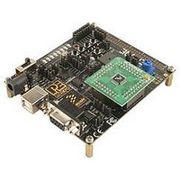
Manufacturer Part Number
DC9S08QE8
Description
DAUGHTER CARD FOR DEMO9S08QB8
Manufacturer
Freescale Semiconductor
Datasheet
1.DC9S08QB8.pdf
(45 pages)
Specifications of DC9S08QE8
Accessory Type
Daughter Card
Silicon Manufacturer
Freescale
Core Architecture
HCS08
Core Sub-architecture
HCS08
Silicon Core Number
MC9S08
Silicon Family Name
Flexis - S08QE
Kit Contents
Board
Features
Four 8x2 Female Connectors
Rohs Compliant
Yes
For Use With/related Products
DEMO9S
Lead Free Status / RoHS Status
Lead free / RoHS Compliant


7.4
7.4.1
28
Figure 7-8: Jumper Settings for Input Signals to P&E’s Embedded Multilink, P&E
Note:
Input and Reset Switches
J11 - P&E’s Logic Analyzer Inputs IN0/IN1
LED PTE6 and LED PTE7 are mapped to QB8 ports PTC6 and PTC7
respectively.
The DEMO9S08QB8 has an option to connect two signals, PTC0 and PTC1,
to the Embedded Multilink for signal processing. The two signals are
connected or disconnected to IN0 or IN1 correspondingly, via jumpers P&E
INPUT_EN (J11).
The DEMO9S08QB8 has 4 switches that are connected to signals PTA2,
PTA3, PTD2, and PTD3 respectively, and are enabled or disabled by the 4
corresponding jumpers KEY_ENABLE (J12).
The DEMO9S08QB8 has one Reset switch and one Reset LED associated
with it. These are enabled or disabled by the two corresponding jumpers
RESET_EN (J18).
The logic analyzer inputs are marked on one side of the J11 jumper. The
inputs allow P&E’s PC-based logic analyzer application to display these
signals in real-time.
Figure 7-7: LED Display Enable Header LED_ENABLE (J9)
By installing both jumpers, the logic analyzer pins IN0 and IN1 will be
connected to PTC0 and PTC1 respectively.
By removing these jumpers IN0 and IN1 will be unconnected. The
user may connect these signals, via wires, to any other signals on the
processor which they wish to view on the PC.
INPUT_EN (J11)
DEMO9S08QB8 User Manual
Related parts for DC9S08QE8
Image
Part Number
Description
Manufacturer
Datasheet
Request
R

Part Number:
Description:
Manufacturer:
Freescale Semiconductor, Inc
Datasheet:
Part Number:
Description:
Manufacturer:
Freescale Semiconductor, Inc
Datasheet:
Part Number:
Description:
Manufacturer:
Freescale Semiconductor, Inc
Datasheet:
Part Number:
Description:
Manufacturer:
Freescale Semiconductor, Inc
Datasheet:
Part Number:
Description:
Manufacturer:
Freescale Semiconductor, Inc
Datasheet:
Part Number:
Description:
Manufacturer:
Freescale Semiconductor, Inc
Datasheet:
Part Number:
Description:
Manufacturer:
Freescale Semiconductor, Inc
Datasheet:
Part Number:
Description:
Manufacturer:
Freescale Semiconductor, Inc
Datasheet:
Part Number:
Description:
Manufacturer:
Freescale Semiconductor, Inc
Datasheet:
Part Number:
Description:
Manufacturer:
Freescale Semiconductor, Inc
Datasheet:
Part Number:
Description:
Manufacturer:
Freescale Semiconductor, Inc
Datasheet:
Part Number:
Description:
Manufacturer:
Freescale Semiconductor, Inc
Datasheet:
Part Number:
Description:
Manufacturer:
Freescale Semiconductor, Inc
Datasheet:
Part Number:
Description:
Manufacturer:
Freescale Semiconductor, Inc
Datasheet:
Part Number:
Description:
Manufacturer:
Freescale Semiconductor, Inc
Datasheet: