PBMCUSLK Freescale Semiconductor, PBMCUSLK Datasheet
PBMCUSLK
Specifications of PBMCUSLK


Related parts for PBMCUSLK

PBMCUSLK Summary of contents
Page 1
... STUDENT LEARNING KIT Prototyping Board with Microcontroller Interface Freescale™ and the Freescale logo are trademarks of Freescale Semiconductor, Inc. All other product or service names are the property of their respective owners © Freescale Semiconductor, Inc. 2006. Document Number: PBMCUSLKUG /REV 1 (PBMCUSLK) PBMCUSLKUG Rev. 1, 7/2007 ...
Page 2
... LCD Port Connectors.................................................................................................................... 14 LCD Contrast ................................................................................................................................ 16 LCD Select.................................................................................................................................... 16 LCD Enable .................................................................................................................................. 17 OSCILLATOR SOCKET .................................................................................................. 17 SWITCHES ..................................................................................................................... 17 PUSHBUTTON SWITCHES ....................................................................................................... 17 DIP SWITCHES ........................................................................................................................... 18 LED’S .............................................................................................................................. 18 KEYPAD.......................................................................................................................... 18 POTENTIOMETER.......................................................................................................... 19 BANANA JACK ............................................................................................................... 19 BNC JACK....................................................................................................................... 19 CONNECTED FEATURES.................................................................................................. 19 POT ................................................................................................................................. 20 PUSH-BUTTON SWITCHES........................................................................................... 20 LED’S .............................................................................................................................. 20 BUZZER .......................................................................................................................... 21 CONNECTED FEATURE ENABLE ................................................................................. 21 COM PORT ......................................................................................................................... 22 2 CONTENTS Freescale Semiconductor ...
Page 3
... Figure 12: COM Port Connector ...............................................................................................22 Figure 14: COM_SEL Option Header .......................................................................................23 Figure 15: MCU_COM Option Header......................................................................................23 Figure 16: USER I/O Signal Breakout – J10, J11 .....................................................................24 Figure 17: MCU_PORT Signal Breakout – J5, J6, J7...............................................................25 Figure 18: Edge Connector – J1..............................................................................................26 Figure 19: NI-ELVIS Signal Breakout – J2, J3, J4 ....................................................................27 Freescale Semiconductor FIGURES 3 ...
Page 4
... Table 4: LED_EN Option Header .............................................................................................18 Table 5: POT Connections .......................................................................................................20 Table 6: PB Switch Connections ..............................................................................................20 Table 7: LED Connections........................................................................................................20 Table 8: User Feature Enable...................................................................................................21 Table 9: UFEA Option Header..................................................................................................21 Date December 5, 2006 July 17, 2007 4 TABLES REVISION Rev 0 Initial Release. 1 Added LCD information (part no., and more info. URLs) Comments Freescale Semiconductor ...
Page 5
... EMC Information on the PBMCUSLK: 1. This product as shipped from the factory with associated power supplies and cables, has been verified to meet with requirements of CE and the FCC as a CLASS A product. ...
Page 6
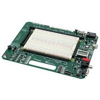
... Freescale MCU development modules in an educational environment. A line of HC(S)12(X), HC(S)08, DSP, and ColdFire modules plug directly into the project board. Other MCU boards can be interfaced directly to the project board by ribbon cable. The PBMCUSLK may also be used as an electronic circuit prototyping environment without MCU support. The project board has been specifically designed for compatibility with the National Instruments Educational Laboratory Virtual Instrumentation Suite (NI-ELVIS) ...
Page 7
... PBMCUSLK to a host PC. OPERATION The PBMCUSLK allows quick and easy prototype of electronic circuits with, or without MCU support. A variety of commonly used circuits are pre-installed, configurable and ready for use. Dual-row header sockets placed around the prototyping area provide convenient access to all Freescale™ ...
Page 8
... Exercise care when configuring power input and output selections to prevent damage to the Input Sources The PBMCUSLK provides the user 4 discrete working voltage levels: 5V, 3.3V, +15V, and - 15V. The 5V and the ±15V rails have multiple input sources while the 3.3V rail is derived from the 5V rail in all configurations ...
Page 9
... NOTE: 3.3V rail is derived from 5V rail for all inputs. Total current available on 3.3V rail is limited by total current available on 5V rail. Freescale Semiconductor Total current drain from USB bus must not exceed 500 mA. Excessive current drain will violate the USB specification. ...
Page 10
... PC. VDD Selection The operating voltage level VDD supplies all on-board logic devices on the PBMCUSLK. An option header allows the user to set VDD at either 5V or 3.3V. When the project board is connected to a wall-plug transformer, voltage regulator VR1 provides the 5V rail and regulator VR2 provides the 3 ...
Page 11
... CAUTION: Exercise care to select the correct operating voltage when interfacing to on-board logic to prevent ±15V Power The PBMCUSLK includes a DC-DC converter at PS1 to supply ±15V for use in analog circuit construction and analysis. PS1 provides a maximum of 50mA on each output. PS1 draws its input from the +5V rail. The option header 15V_EN output if not needed ...
Page 12
... Damage to both the project board and Integrated USB BDM The PBMCUSLK board features an integrated USB Background Debug Mode (BDM) from P&E Microcomputer Systems. The integrated BDM possesses all the necessary signals to support application development and debugging. ...
Page 13
... BDM Voltage The integrated BDM is designed to interface with either 5V or 3.3V circuits. The VDD level selected on the PBMCUSLK is fed back to the BDM to set output drive levels. The VDD level is selected by VDD_SEL(JP3) option header. Further details on operating voltage selection may be found in the POWER section above. ...
Page 14
... User I/O The PBMCUSLK provides an array of User I/O to allow connection of auxiliary components such as signal input, test equipment, Keypads, or LCD displays. Many of these user features are by default enabled, but can be disconnected through jumper settings. describes each of the features in detail, for more information on configuring these features please view the Connected Features section ...
Page 15
... LCD_D4 11 LCD_D5 12 LCD_D6 13 LCD_D7 14 Freescale Semiconductor VDD SPI data bit definitions to LCD Port: LCD_D[7..4] – LCD data bits D[3..0] RS DB[3..0] – Unused, 10K ohm pull-downs installed EN R/W – Read/Write pin, set to 0 volts, Read only DB1 EN – LCD enable input LCD enable DB3 CONTRAST – ...
Page 16
... LCD Contrast The PBMCUSLK offers two methods for controlling the LCD panel contrast, fixed or adjustable, controlled through jumper CONTRAST(JP12) as illustrated in figure 8. provides near maximum contrast and supports all STN, Reflective, type LCD panels. The fixed mode is pre-set to a contrast easily viewable in ambient, indoor lighting. The adjustable option allows the use on the project board potentiometer to vary the contrast voltage applied to the LCD panel ...
Page 17
... Oscillator Output at Full Amplitude – 5V OFF Oscillator Output at Reduced Amplitude – 3.3V Switches The PBMCUSLK provides two types of switches for use as input devices. Eight normally open push button switches voltage level while in the inactive state. PUSHBUTTON SWITCHES Each push button switch is configured for active-low operation. When pressed (closed) the associated signal line is pulled to GND through a 1 kΩ ...
Page 18
... I/O SW[1..7] located adjacent to the breadboard. LED’s The PBMCUSLK provides 8, green LED’s, for use as output indicators. configured for active-high operation. Each LED is individually driven by an ACT buffer allowing either 5V or 3.3V input levels. The input level is determined by VDD selection. A 10K ohm resistor holds each buffer input low to prevent inadvertent LED activation ...
Page 19
... BNC Jack The PBMCUSLK provides one BNC jack for use as auxiliary I/O. This connector may be used for auxiliary signal input or for signal output to test equipment. The center conductor (BNC+) and shield (BNC-) are routed separately to the User I/O Signal Breakout connector labeled USER I/O BNC[+/-] located adjacent to the breadboard area ...
Page 20
... MCU control. An option header at UFEA isolates this enable signal allowing the user to apply the GPIO signal for other uses. Table 7: LED Connections FEATURE CONNECTION LED1 VALUE MCU_PORT – 33 LED2 VALUE MCU_PORT – 35 LED3 VALUE MCU_PORT – 37 LED4 VALUE MCU_PORT - 39 LED ENABLE MCU_PORT - 34 OPTION JUMPER UFEA -3 (LED) 20 Freescale Semiconductor ...
Page 21
... Buzzer The PBMCUSLK features an external drive buzzer for audible applications. The buzzer is connected to a TIMER / PWM port on all current MCU modules. The buzzer is connected directly to the MCU _PORT connector at MCU_PORT – 13 and does not require an enable signal similar to the other Connected Features. The buzzer is connected to the MCU_PORT through an option header at UFEA -2 (PB) ...
Page 22
... DB9 Connector A single DB9 connector shown in figure 12 is provided to support communications applications development on the PBMCUSLK. Signals from the DB9 connector are routed directly to the breakout connector labeled COMM DSUB[1..9] located adjacent to the breadboard. allows implementation of communication protocols not supported on the PBMCUSLK. ...
Page 23
... To ease application development, communications signals TX and RX are connected the MCU_PORT connect at pins 5 & 7 respectively. This simplifies cable routing when using the PBMCUSLK and an attached module. The MCU_COM option header is used to route these signals from the on-board transceiver to the MCU_PORT headers. To use the signals as general-purpose I/O, simply remove the shunts at the MCU_COM option header as described in figure 15 ...
Page 24
... Signal Breakout An important feature of the PBMCUSLK is the large, centrally located, breadboard area. Dual-row socket headers strategically placed around the breadboard provide signal access to the on-board circuits. Signal breakouts may be grouped into 3 broad categories: MCU Access Signals, User I/O Signals, and NI-ELVIS Signals USER I/O User I/O signal breakout connectors provide access to all on-board components ...
Page 25
... MCU_PORT A unique feature of the PBMCUSLK is the ability to interface directly with a line of MCU Development Boards from Axiom Manufacturing. directly into the MCU_PORT or connect through a ribbon cable. The signals originating at the MCU_PORT connector are routed to two sets of dual-row socket headers located at both ends of the breadboard ...
Page 26
... NI-ELVIS Interface The NI-ELVIS interface consists of a PCI style connector located at J1 and 3 dual-row socket headers. Connector J1 connects the PBMCUSLK directly to the NI-ELVIS workstation. All NI- ELVIS signals are routed to a signal breakout connector conveniently located adjacent to the breadboard. Refer to the NI-ELVIS User Guide for details on the functioning of the NI-ELVIS platform. In the figure below, all ‘ ...
Page 27
... FUNC OUT 27 28 SYNC OUT TRIGGER 39 40 AISENSE 41 42 AIGND 43 44 ACH0 ACH0 ACH1 ACH1 ACH2 ACH2 ACH3 ACH3 ACH4+ Freescale Semiconductor ACH4 ACH5 ACH5 FREQ_OUT 9 10 CTR0_SOURCE 11 12 CTR0_GATE 13 14 CTR0_OUT 15 16 CTR1_SOURCE 17 18 CTR1_GATE 19 20 CTR1_OUT RESERVED 27 28 SCAN CLK ...
Page 28
... Measure 3.3VDC between pins VR2-2 and VR2-3 LED’s on the MCU Development Module don’t light • Make sure the module is properly connected to the PBMCUSLK - 2 • Make sure a power cord is not connected to the module • Make sure the MODULE POWER option jumpers are installed • ...
Page 29
... APPENDIX A SILKSCREEN Freescale Semiconductor 29 ...
Page 30
... Axiom Manufacturing 2813 Industrial Lane Garland, Tx. 75041 Phone: 972-926-9303 Web: www.axman.com Document Number: XX0000 PBMCUSLKUG RTYPEev. X Rev. 1 09/2005 07/2007 Information in this document is provided solely to enable system and software implementers to use Freescale Semiconductor products. There are no express or implied copyright licenses granted hereunder to design or fabricate any integrated circuits or integrated circuits based on the information in this document ...