EPC9001 EPC, EPC9001 Datasheet - Page 3
EPC9001
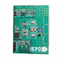
Manufacturer Part Number
EPC9001
Description
BOARD DEV FOR EPC1015 40V GAN
Manufacturer
EPC
Datasheet
1.EPC1015.pdf
(4 pages)
Specifications of EPC9001
Design Resources
EPC9001 Schematic EPC9001 Gerber Files EPC9001 Bill Of Materials
Main Purpose
Power Management, Half H-Bridge Driver (External FET)
Utilized Ic / Part
EPC1015
Primary Attributes
40V, 15A Max Output GaNFET Capability
Secondary Attributes
GaNFET Driver Circuit Uses 7 ~ 12V
Kit Contents
(2) 917-1009-1-ND - TRANS GAN 40V 33A BUMPED DIE
Lead Free Status / RoHS Status
Contains lead / RoHS non-compliant
Embedded
-
Other names
917-1010


DATASHEET
EPC – EFFICIENT POWER CONVERSION CORPORATION | WWW.EPC-CO.COM | COPYRIGHT 2010 |
TAPE AND REEL CONFIGURATION
4mm pitch, 12mm wide tape on 7” reel
10
10
10
10
10
-1
-2
-20
0
2
1
Figure 9: Normalized Threshold Voltage
0
Figure 7: Reverse Drain-Source Characteristics
I
D
= 9 mA
7” reel
0
0.5
25˚C
125˚C
20
V
T
1
J
SD
– Junction Temperature ( ˚C )
– Source to Drain Voltage (V)
40
a
1.5
Dimension (mm) target min
b
c (see note)
f (see note)
60
c
a
b
d
e
g
2
80
d
2.5
12.0 11.7 12.3
1.75 1.65 1.85
5.50 5.45 5.55
4.00 3.90 4.10
4.00 3.90 4.10
2.00 1.95 2.05
100
1.5
EPC1015
1.5
e
120
3
max
1.6
140
3.5
f
Note: Pocket position is relative to the sprocket hole
measured as true position of the pocket, not the pocket hole
g
.018
.016
.014
.012
.008
.006
.004
.002
.02
.01
0
-20
0
Figure 8: Normalized On Resistance Vs Temperature
Figure 10: Gate Current
Loaded Tape Feed Direction
I
V
D
GS
= 33 A
= 5 V
0
25˚C
125˚C
1
Die is placed into pocket
20
T
V
J
GS
– Junction Temperature ( ˚C )
bump side down
(face side down)
2
– Gate-to-Source Voltage (V)
40
60
3
80
4
under this
Gate Pad
orientation
bump is
corner
100
Die
dot
5
120
EPC1015
| PAGE 3
140
6
Related parts for EPC9001
Image
Part Number
Description
Manufacturer
Datasheet
Request
R

Part Number:
Description:
Multi Video Capture Ports Embedded PC
Manufacturer:
PROTECHSYSTEMS [Protech Systems Co., Ltd.]
Datasheet:

Part Number:
Description:
IC CONFIG DEVICE 1MBIT 8-DIP
Manufacturer:
Altera
Datasheet:

Part Number:
Description:
IC CONFIG DEVICE 1.6MBIT 20-PLCC
Manufacturer:
Altera
Datasheet:
Part Number:
Description:
IC CONFIG DEVICE 1.6MBIT 20-PLCC
Manufacturer:
Altera
Datasheet:

Part Number:
Description:
IC CONFIG DEVICE 1.6MBIT 32-TQFP
Manufacturer:
Altera
Datasheet:
Part Number:
Description:
IC CONFIG DEVICE 1.6MBIT 32-TQFP
Manufacturer:
Altera
Datasheet:
Part Number:
Description:
IC CONFIG DEVICE 1.6MBIT 20-PLCC
Manufacturer:
Altera
Datasheet:
Part Number:
Description:
IC CONFIG DEVICE 1.6MBIT 20-PLCC
Manufacturer:
Altera
Datasheet:

Part Number:
Description:
IC CONFIG DEVICE 8MBIT 100-PQFP
Manufacturer:
Altera
Datasheet:
Part Number:
Description:
IC CONFIG DEVICE 1.6MBIT 32-TQFP
Manufacturer:
Altera
Datasheet:
Part Number:
Description:
IC CONFIG DEVICE 1.6MBIT 32-TQFP
Manufacturer:
Altera
Datasheet:
Part Number:
Description:
IC CONFIG DEVICE 16MBIT 100-PQFP
Manufacturer:
Altera
Datasheet:
Part Number:
Description:
IC CONFIG DEVICE 16MBIT 100-PQFP
Manufacturer:
Altera
Datasheet:
Part Number:
Description:
IC CONFIG DEVICE 16MBIT 100-PQFP
Manufacturer:
Altera
Datasheet:

Part Number:
Description:
IC CONFIG DEVICE 16MBIT 88-UBGA
Manufacturer:
Altera
Datasheet: