MCP1631RD-MCC2 Microchip Technology, MCP1631RD-MCC2 Datasheet - Page 16
MCP1631RD-MCC2
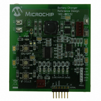
Manufacturer Part Number
MCP1631RD-MCC2
Description
REFERENCE DESIGN MCP1631HV
Manufacturer
Microchip Technology
Datasheets
1.MCP1631VHVT-330EST.pdf
(34 pages)
2.MCP1631HV-330EST.pdf
(54 pages)
3.MCP1631RD-MCC2.pdf
(20 pages)
4.MCP1631RD-MCC2.pdf
(328 pages)
Specifications of MCP1631RD-MCC2
Main Purpose
Power Management, Battery Charger
Embedded
Yes, MCU, 8-Bit
Utilized Ic / Part
MCP1631HV, PIC16F883
Primary Attributes
1 ~ 2 Cell- Li-Ion, 1 ~ 5 Cell- NiCd/NiMH, 1 ~ 2 1W LEDs
Secondary Attributes
Status LEDs
Silicon Manufacturer
Microchip
Application Sub Type
Battery Charger
Kit Application Type
Power Management - Battery
Silicon Core Number
MCP1631HV, PIC16F883
Kit Contents
Board
Lead Free Status / RoHS Status
Lead free / RoHS Compliant
Lead Free Status / RoHS Status
Lead free / RoHS Compliant


MCP1631/HV/MCP1631V/VHV
3.7
Quiet or analog ground, connect to analog ground
plane to minimize noise on sensitive MCP1631
circuitry.
3.8
No connection.
3.9
High voltage input for MCP1631HV/MCP1631VHV
devices, operates from 3.5V to 16V input supply.
3.10
Analog bias input, minimum 3.0V to 5.5V operation for
MCP1631/MCP1631V devices.
3.11
Regulated V
M C P 1 6 3 1 H V / M C P 1 6 3 1 V H V a n d e x t e r n a l
microcontroller, supplies up to 250 ma of bias current at
3.3V or 5.0V regulated low drop out rail.
3.12
Voltage sense amplifier (A3) input, connect to high
impedance battery voltage resistor divider to sense
battery voltage with minimal loading.
3.13
Connect to SEPIC secondary side sense resistor to
develop a regulated current source used to charge
multi-chemistry batteries.
3.14
Voltage
microcontroller analog to digital converter to measure
battery voltage.
DS22063B-page 16
Analog Ground (A
No Connection (NC)
Input Voltage (V
Analog supply Input (A
Analog Supply Output (A
Voltage Sense Input (VS
Current Sense Input (IS
Voltage Sense Output (VS
sense
DD
output used to power internal
amplifier
IN
output,
)
GND
)
VDD_IN
IN
IN
connect
VDD_OUT
)
)
OUT
)
)
)
to
3.15
Current sense amplifier output, connect to error
amplifier (A1) inverting input (FB) to regulate SEPIC
output current.
3.16
Error amplifier (A1) output, connect control loop
compensation from FB input to COMP output pin.
3.17
Error amplifier input (A1), connect to current sense
output amplifier (A2) to regulate current.
3.18
For MCP1631/MCP1631HV applications, connect to
low side current sense of SEPIC switch for current
mode control and peak current limit. For MCP1631/
MCP1631HV application, connect artificial ramp
voltage to V
3.19
Power V
to +5.0V or +3.3V supply for driving external MOSFET.
3.20
High current driver output used to drive external
MOSFET at high frequency, capable of 1A peak
currents with +5.0V P
3.21
There is an internal electrical connection between the
Exposed Thermal Pad (EP) and the A
must be connected to the same potential on the Printed
Circuit Board (PCB).
DD
Current Sense Output (IS
Error Amplifier Output (COMP)
Feedback (FB)
Current Sense or Voltage Ramp
(CS/V
Power VDD (P
External Driver (V
Exposed PAD 4x4 QFN (EP)
input, V
RAMP
RAMP
input for voltage mode PWM control.
EXT
VDD
)
gate drive supply input, connect
© 2008 Microchip Technology Inc.
.
VDD
)
EXT
)
GND
OUT
pin; they
)
Related parts for MCP1631RD-MCC2
Image
Part Number
Description
Manufacturer
Datasheet
Request
R

Part Number:
Description:
REFERENCE DESIGN FOR MCP1631HV
Manufacturer:
Microchip Technology
Datasheet:

Part Number:
Description:
REF DES BATT CHARG OR LED DRIVER
Manufacturer:
Microchip Technology
Datasheet:

Part Number:
Description:
Manufacturer:
Microchip Technology Inc.
Datasheet:
Part Number:
Description:
Manufacturer:
Microchip Technology Inc.
Datasheet:
Part Number:
Description:
Manufacturer:
Microchip Technology Inc.
Datasheet:
Part Number:
Description:
Manufacturer:
Microchip Technology Inc.
Datasheet:
Part Number:
Description:
Manufacturer:
Microchip Technology Inc.
Datasheet:
Part Number:
Description:
Manufacturer:
Microchip Technology Inc.
Datasheet:
Part Number:
Description:
Manufacturer:
Microchip Technology Inc.
Datasheet:
Part Number:
Description:
Manufacturer:
Microchip Technology Inc.
Datasheet: