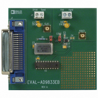
EVAL-AD9833EBZ Analog Devices Inc, EVAL-AD9833EBZ Datasheet - Page 21
EVAL-AD9833EBZ
Manufacturer Part Number
EVAL-AD9833EBZ
Description
BOARD EVAL FOR AD9833
Manufacturer
Analog Devices Inc
Datasheet
1.AD9833BRMZ.pdf
(24 pages)
Specifications of EVAL-AD9833EBZ
Main Purpose
Timing, Direct Digital Synthesis (DDS)
Embedded
No
Utilized Ic / Part
AD9833
Primary Attributes
10-Bit DAC, 28-Bit Tuning Word Width
Secondary Attributes
25MHz, Graphical User Interface, 2.3 V ~ 5.5 V
Lead Free Status / RoHS Status
Lead free / RoHS Compliant
Other names
EVAL-AD9833EB
EVAL-AD9833EB
EVAL-AD9833EB
Available stocks
Company
Part Number
Manufacturer
Quantity
Price
Company:

Part Number:
EVAL-AD9833EBZ
Manufacturer:
Analog Devices Inc
Quantity:
135


AD9833 TO 80C51/80L51 INTERFACE
Figure 31 shows the serial interface between the AD9833 and
the 80C51/80L51 microcontroller. The microcontroller is operated
in Mode 0 so that TxD of the 80C51/80L51 drives SCLK of the
AD9833, while RxD drives the serial data line SDATA. The
FSYNC signal is again derived from a bit programmable pin on
the port (P3.3 being used in Figure 31). When data is to be
transmitted to the AD9833, P3.3 is taken low. The 80C51/80L51
transmits data in 8-bit bytes, thus only eight falling SCLK edges
occur in each cycle. To load the remaining 8 bits to the AD9833,
P3.3 is held low after the first 8 bits have been transmitted, and
a second write operation is initiated to transmit the second byte
of data. P3.3 is taken high following the completion of the second
write operation. SCLK should idle high between the two write
operations. The 80C51/80L51 outputs the serial data in a format
that is LSB first. The AD9833 accepts MSB first (the 4 MSBs
being the control information, the next 4 bits being the address,
while the 8 LSBs contain the data when writing to a destination
register). Therefore, the transmit routine of the 80C51/80L51
must take this into account and rearrange the bits so that the
MSB is output first.
*ADDITIONAL PINS OMITTED FOR CLARITY.
80C51/80L51*
Figure 31. 80C51/80L51 to AD9833 Interface
P3.3
RxD
TxD
FSYNC
SDATA
SCLK
AD9833*
Rev. C | Page 21 of 24
AD9833 TO DSP56002 INTERFACE
Figure 32 shows the interface between the AD9833 and the
DSP56002. The DSP56002 is configured for normal mode
asynchronous operation with a gated internal clock (SYN = 0,
GCK = 1, SCKD = 1). The frame sync pin is generated internally
(SC2 = 1), the transfers are 16 bits wide (WL1 = 1, WL0 = 0),
and the frame sync signal frames the 16 bits (FSL = 0). The frame
sync signal is available on SC2, but it needs to be inverted before
being applied to the AD9833. The interface to the DSP56000/
DSP56001 is similar to that of the DSP56002.
*ADDITIONAL PINS OMITTED FOR CLARITY.
DSP56002*
Figure 32. DSP56002 to AD9833 Interface
SCK
STD
SC2
FSYNC
SDATA
SCLK
AD9833*
AD9833
Related parts for EVAL-AD9833EBZ
Image
Part Number
Description
Manufacturer
Datasheet
Request
R


Part Number:
Description:
BOARD EVAL FOR SI270X-A
Manufacturer:
Silicon Laboratories Inc
Datasheet:

Part Number:
Description:
BUCK CONV REF DESIGN KIT IP1201
Manufacturer:
International Rectifier
Datasheet:
Part Number:
Description:
BOARD DEMO SYNC DUAL BUCK CNVTER
Manufacturer:
International Rectifier
Datasheet:
Part Number:
Description:
BOARD DEMO SYNC BUCK CONVETER
Manufacturer:
International Rectifier
Datasheet:

Part Number:
Description:
EVALBOARD/EB Omnidirectional microphone - Analog
Manufacturer:
Analog Devices
Datasheet:
Part Number:
Description:
EVALBOARD/EB Omnidirectional microphone - Analog
Manufacturer:
Analog Devices
Datasheet:


Part Number:
Description:
BOARD EVAL LED DRIVER LT3756
Manufacturer:
Linear Technology
Datasheet:

Part Number:
Description:
BOARD EVAL FOR AD7741/7742
Manufacturer:
Analog Devices Inc
Datasheet:

Part Number:
Description:
±1.7g Dual-Axis IMEMS Accelerometer Evaluation Board
Manufacturer:
Analog Devices Inc
Datasheet:

Part Number:
Description:
IC MULTIPLIER ANALOG 8-SOIC T/R
Manufacturer:
Analog Devices Inc
Datasheet:

Part Number:
Description:
IC ANALOG MULTIPLIER 8-DIP
Manufacturer:
Analog Devices Inc
Datasheet:
Part Number:
Description:
IC ANALOG MULTIPLIER 8-SOIC
Manufacturer:
Analog Devices Inc
Datasheet:
Part Number:
Description:
IC ANALOG MULTIPLIER 8-DIP
Manufacturer:
Analog Devices Inc
Datasheet: